ADXL345BCCZ-RL7 Analog Devices Inc, ADXL345BCCZ-RL7 Datasheet - Page 17
ADXL345BCCZ-RL7
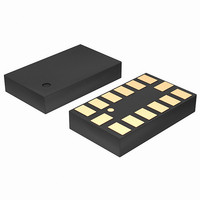
Manufacturer Part Number
ADXL345BCCZ-RL7
Description
Digital Output Three-Axis XL 1500pc RL
Manufacturer
Analog Devices Inc
Series
iMEMS®r
Datasheet
1.EVAL-ADXL345Z.pdf
(40 pages)
Specifications of ADXL345BCCZ-RL7
Design Resources
Sensing Low-g Acceleration Using ADXL345 Digital Accelerometer Connected to ADuC7024 (CN0133)
Axis
X, Y, Z
Acceleration Range
±2g, 4g, 8g, 16g
Sensitivity
256LSB/g, 128LSB/g, 64LSB/g, 32LSB/g
Voltage - Supply
2 V ~ 3.6 V
Output Type
Digital
Bandwidth
6.25Hz ~ 3.2kHz Selectable
Interface
I²C, SPI
Mounting Type
Surface Mount
Package / Case
14-LGA
Lead Free Status / RoHS Status
Lead free / RoHS Compliant
For Use With
EVAL-ADXL345Z - BOARD EVALUATION FOR ADXL345EVAL-ADXL345Z-S - BOARD SATELLITE FOR ADXL345Z-MEVAL-ADXL345Z-M - BOARD EVAL FOR ADXL345
Lead Free Status / RoHS Status
Lead free / RoHS Compliant
Other names
ADXL345BCCZ-RL7TR
Available stocks
Company
Part Number
Manufacturer
Quantity
Price
Company:

Part Number:
ADXL345BCCZ-RL7
Manufacturer:
POWER
Quantity:
14 300


Table 9. SPI Digital Input/Output
Parameter
Digital Input
Low Level Input Voltage (V
High Level Input Voltage (V
Low Level Input Current (I
High Level Input Current (I
Digital Output
Low Level Output Voltage (V
High Level Output Voltage (V
Low Level Output Current (I
High Level Output Current (I
Pin Capacitance
1
Table 10. SPI Timing (T
Parameter
f
t
t
t
t
t
t
t
t
t
t
t
t
1
2
3
4
SCLK
SCLK
DELAY
QUIET
DIS
CS,DIS
S
M
SETUP
HOLD
SDO
R
F
Limits based on characterization results, not production tested.
The CS , SCLK, SDI, and SDO pins are not internally pulled up or down; they must be driven for proper operation.
Limits based on characterization results, characterized with f
The timing values are measured corresponding to the input thresholds (V
Output rise and fall times measured with capacitive load of 150 pF.
4
4
Min
200
5
5
150
0.3 × t
0.3 × t
5
5
Limit
SCLK
SCLK
A
IL
IH
IL
)
= 25°C, V
IH
OL
)
)
OH
OL
2, 3
)
OH
)
)
)
)
Max
5
10
40
20
20
S
= 2.5 V,
Unit
MHz
ns
ns
ns
ns
ns
ns
ns
ns
ns
ns
ns
ns
VDD I/O
Description
SPI clock frequency
1/(SPI clock frequency) mark-space ratio for the SCLK input is 40/60 to 60/40
CS falling edge to SCLK falling edge
SCLK rising edge to CS rising edge
CS rising edge to SDO disabled
CS deassertion between SPI communications
SCLK low pulse width (space)
SCLK high pulse width (mark)
SDI valid before SCLK rising edge
SDI valid after SCLK rising edge
SCLK falling edge to SDO/SDIO output transition
SDO/SDIO output high to output low transition
SDO/SDIO output low to output high transition
SCLK
= 1.8 V)
= 5 MHz and bus load capacitance of 100 pF; not production tested.
Test Conditions
V
V
I
I
V
V
f
OL
OH
IN
IN
IN
OL
OH
= 1 MHz, V
= 10 mA
= −4 mA
= V
= 0 V
= V
= V
Rev. B | Page 17 of 40
DD I/O
OL, max
OH, min
IL
1
and V
IN
IH
) given in Table 9.
= 2.5 V
Min
0.7 × V
−0.1
0.8 × V
10
DD I/O
DD I/O
Limit
Max
0.3 × V
0.1
0.2 × V
−4
8
1
DD I/O
DD I/O
ADXL345
Unit
V
V
μA
μA
V
V
mA
mA
pF
Related parts for ADXL345BCCZ-RL7
Image
Part Number
Description
Manufacturer
Datasheet
Request
R

Part Number:
Description:
±1.7g Dual-Axis IMEMS Accelerometer Evaluation Board
Manufacturer:
Analog Devices Inc
Datasheet:

Part Number:
Description:
Inertial Sensor Evaluation System
Manufacturer:
Analog Devices Inc
Datasheet:
Part Number:
Description:
Manufacturer:
Analog Devices Inc
Datasheet:
Part Number:
Description:
Manufacturer:
Analog Devices Inc
Datasheet:
Part Number:
Description:
Manufacturer:
Analog Devices Inc
Datasheet:
Part Number:
Description:
Manufacturer:
Analog Devices Inc
Datasheet:
Part Number:
Description:
Manufacturer:
Analog Devices Inc
Datasheet:
Part Number:
Description:
Manufacturer:
Analog Devices Inc
Datasheet:
Part Number:
Description:
Manufacturer:
Analog Devices Inc
Datasheet:
Part Number:
Description:
Manufacturer:
Analog Devices Inc
Datasheet:
Part Number:
Description:
Manufacturer:
Analog Devices Inc
Datasheet:
Part Number:
Description:
Manufacturer:
Analog Devices Inc
Datasheet:
Part Number:
Description:
Manufacturer:
Analog Devices Inc
Datasheet: