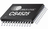
CS4525-CNZR Cirrus Logic Inc, CS4525-CNZR Datasheet - Page 54

CS4525-CNZR
Manufacturer Part Number
CS4525-CNZR
Description
IC PWM Controller+power Stage
Manufacturer
Cirrus Logic Inc
Series
Popguard®r
Type
Class Dr
Datasheet
1.CS4525-CNZ.pdf
(98 pages)
Specifications of CS4525-CNZR
Output Type
2-Channel (Stereo) or 4-Channel (Quad)
Max Output Power X Channels @ Load
30W x 1 @ 4 Ohm; 15W x 2 @ 8 Ohm
Voltage - Supply
8 V ~ 18 V
Features
ADC, Depop, I²C, I²S, Mute, PWM, Short-Circuit and Thermal Protection, Volume Control
Mounting Type
Surface Mount
Package / Case
48-QFN
Lead Free Status / RoHS Status
Lead free / RoHS Compliant
For Use With
598-1586 - REFERENCE BOARD FOR CS4525 PWM
Lead Free Status / RoHS Status
Lead free / RoHS Compliant
Available stocks
Company
Part Number
Manufacturer
Quantity
Price
Part Number:
CS4525-CNZR
Manufacturer:
CIRRUSLOGICINC
Quantity:
20 000
54
6.2
6.2.1
6.2.2
Hardware Mode
A limited feature set is available when the CS4525 powers up in hardware mode. The available features are
described in the following sections. All device configuration is achieved via hardware control input pins.
6.2.2.1
System Clocking
In hardware mode, the CS4525 must be clocked by a stable external clock source input on the SYS_CLK
pin. This input clock is used to synchronize the input serial audio signals with the internal clock domain
and to clock the internal digital processing, sample-rate converter, and PWM modulators. It is also used
to determine the sample rate of the serial audio input signals in order to automatically configure the vari-
ous internal filter coefficients.
To ensure proper operation, the CS4525 must be informed of the nominal frequency of the supplied
SYS_CLK signal via the ClkFreq0 hardware control pin. This pin must be set to the appropriate level be-
fore the RST signal is released to initiate a power-up sequence. The ClkFreq1 pin must always be con-
nected to DGND. The nominal clock frequencies indicated by the state of the ClkFreq0 pin are shown in
Table 13
cy range specifications.
WARNING: The SYS_CLK signal must never be removed or stopped while the RST pin is high and any
of the power output stages are connected to a load. Doing so may result in permanent damage to the
CS4525 and connected transducers.
Figure 22
Power-Up and Power-Down
The CS4525 will remain in a completely powered-down state until the RST pin is brought high.
1. Apply the SYS_CLK signal.
2. Hold RST low until the power supplies and the input SYS_CLK signal are stable.
3. Bring RST high.
Hardware mode will be entered after approximately 10 ms.
ClkFreq1
Low
Low
below. See the
below demonstrates a typical clocking configuration using the SYS_CLK input.
Power-Up Sequence
Clock
Figure 22. Typical SYS_CLK Input Clocking Configuration
SYS_CLK Switching Specifications
ClkFreq0
High
Low
Table 13. SYS_CLK Frequency Selection
Clock_In
DSP
Reset_Out
Nominal SYS_CLK Frequency
table on
RST
18.432 MHz
24.576 MHz
page 23
SYS_CLK
CS4525
for complete input frequen-
XTO
XTI
CS4525
DS726PP3


