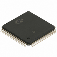
CY7B994V-2AXIT Cypress Semiconductor Corp, CY7B994V-2AXIT Datasheet - Page 7

CY7B994V-2AXIT
Manufacturer Part Number
CY7B994V-2AXIT
Description
IC,Eighteen Distributed-Output Clock Driver,QFP,100PIN,PLASTIC
Manufacturer
Cypress Semiconductor Corp
Series
RoboClock™r
Type
Clock Buffer, Fanout Distributionr
Datasheet
1.CY7B993V-2AXC.pdf
(18 pages)
Specifications of CY7B994V-2AXIT
Pll
Yes
Input
LVPECL, LVTTL
Output
LVTTL
Number Of Circuits
1
Ratio - Input:output
4:18
Differential - Input:output
No/No
Frequency - Max
200MHz
Divider/multiplier
Yes/Yes
Voltage - Supply
2.97 V ~ 3.63 V
Operating Temperature
-40°C ~ 85°C
Mounting Type
Surface Mount
Package / Case
100-LQFP
Frequency-max
200MHz
Lead Free Status / RoHS Status
Lead free / RoHS Compliant
Available stocks
Company
Part Number
Manufacturer
Quantity
Price
Company:
Part Number:
CY7B994V-2AXIT
Manufacturer:
Cypress Semiconductor Corp
Quantity:
10 000
Table 2. Frequency Range Select
Time Unit Definition
Selectable skew is in discrete increments of time unit (t
value of a t
nominal output frequency. The equation to be used to determine
the t
t
N is a multiplication factor which is determined by the FS setting.
f
Table 3. N Factor Determination
Divide and Phase Select Matrix
The Divide and Phase Select Matrix is comprised of five
independent banks: four banks of clock outputs and one bank for
feedback. Each clock output bank has two pairs of low-skew,
high-fanout output buffers ([1:4]Q[A:B][0:1]), two phase function
select inputs ([1:4]F[0:1]), two divider function selects
([1:4]DS[0:1]), and one output disable (DIS[1:4]).
The feedback bank has one pair of low-skew, high-fanout output
buffers (QFA[0:1]). One of these outputs may connect to the
selected feedback input (FBK[A:B]±). This feedback bank also
has one phase function select input (FBF0), two divider function
selects FSDS[0:1], and one output disable (FBDIS).
The phase capabilities that are chosen by the phase function
select pins are shown in
bank are shown in
Document #: 38-07127 Rev. *I
LOW
MID
HIGH
LOW
MID
HIGH
U
NOM
Notes
2. The level to be set on FS is determined by the “nominal” operating frequency (f
3. BK1, BK2 denotes following the skew setting of Bank1 and Bank2, respectively.
FS
= 1/(f
FS
the output is operating in the undivided mode. The REF and FB are at f
U
[2]
is nominal frequency of the device. N is defined in
value is as follows:
NOM
U
64
32
16
N
*N)
is determined by the FS setting and the maximum
Min
12
24
48
f
CY7B993V
CY7B993V
NOM
which t
f
Table
NOM
(MHz)
15.625
31.25
62.5
(MHz) at
Table
U
5.
Max
100
=1.0 ns
26
52
4. The divide capabilities for each
32
16
N
8
Min
24
48
96
f
CY7B994V
CY7B994V
which t
NOM
f
NOM
(MHz)
31.25
62.5
125
(MHz) at
U
Max
=1.0 ns
100
200
52
Table
U
). The
NOM
3.
when the output connected to FB is undivided.
NOM
Table 4. Output Skew Select Function
Table 5. Output Divider Function
Figure 3
outputs. All times are measured with respect to REF with the
output used for feedback programmed with 0t
naturally aligns the rising edge of the FB input and REF input. If
the output used for feedback is programmed to another skew
position, then the whole t
example, if the output used for feedback is programmed to shift
–8t
an output programmed with 8t
16t
) of the V
[1:4]DS1
[1:4]F1
FBDS1
HIGH
HIGH
HIGH
LOW
LOW
LOW
MID
MID
MID
HIGH
HIGH
HIGH
LOW
LOW
LOW
and
MID
MID
MID
U
U
Function
, then the whole matrix is shifted forward in time by 8t
Selects
with respect to REF.
Function
Selects
CO
illustrates the timing relationship of programmable skew
[1:4]F0
and Phase Generator. f
FBF0
HIGH
HIGH
HIGH
LOW
LOW
LOW
and
MID
MID
MID
[1:4]DS0
FBDS0
HIGH
HIGH
HIGH
LOW
LOW
LOW
and
MID
MID
MID
Bank1 Bank2 Bank3 Bank4
–4t
–3t
–2t
–1t
+1t
+2t
+3t
+4t
0t
Bank1 Bank2 Bank3 Bank4
U
U
U
U
U
U
U
U
U
/10
/12
/1
/2
/3
/4
/5
/6
/8
U
CY7B993V, CY7B994V
matrix shifts with respect to REF. For
Output Skew Function
NOM
Output Divider Function
–4t
–3tu
–2t
–1t
+1t
+2t
+3t
+4t
0t
U
U
always appears on an output when
/10
/12
U
U
U
U
U
U
U
/4
/5
/6
/1
/2
/3
/8
of skew is effectively skewed
BK1
BK2
–8t
–7t
–6t
+6t
+7t
+8t
0t
/10
/12
U
/1
/2
/3
/4
/5
/6
/8
U
U
U
U
U
U
[3]
[3]
RoboClock
BK1
BK2
+6t
+7t
+8t
–8t
–7t
–6t
U
0t
/10
/12
/1
/2
/3
/4
/5
/6
/8
U
skew. The PLL
U
U
U
U
U
U
[3]
[3]
Page 7 of 18
Feed-
Feed-
Bank
back
Bank
back
+4t
–4t
NA
NA
NA
0tu
NA
NA
NA
/10
/12
/1
/2
/3
/4
/5
/6
/8
U
. Thus
U
U
[+] Feedback


