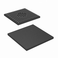
CY7C057V-12BBC Cypress Semiconductor Corp, CY7C057V-12BBC Datasheet - Page 11

CY7C057V-12BBC
Manufacturer Part Number
CY7C057V-12BBC
Description
IC,SRAM,32KX36,CMOS,BGA,172PIN,PLASTIC
Manufacturer
Cypress Semiconductor Corp
Datasheet
1.CY7C057V-15BBC.pdf
(26 pages)
Specifications of CY7C057V-12BBC
Format - Memory
RAM
Memory Type
SRAM - Dual Port, Asynchronous
Memory Size
1.152M (32K x 36)
Speed
12ns
Interface
Parallel
Voltage - Supply
3 V ~ 3.6 V
Operating Temperature
0°C ~ 70°C
Package / Case
172-LFBGA
Lead Free Status / RoHS Status
Contains lead / RoHS non-compliant
Available stocks
Company
Part Number
Manufacturer
Quantity
Price
Company:
Part Number:
CY7C057V-12BBC
Manufacturer:
CY
Quantity:
250
Company:
Part Number:
CY7C057V-12BBC
Manufacturer:
CYPRESS
Quantity:
300
Company:
Part Number:
CY7C057V-12BBC
Manufacturer:
Cypress Semiconductor Corp
Quantity:
10 000
Part Number:
CY7C057V-12BBC
Manufacturer:
CYPRESS/赛普拉斯
Quantity:
20 000
Switching Characteristics
Data Retention Mode
The CY7C056V and CY7C057V are designed with battery
backup in mind. Data retention voltage and supply current are
guaranteed over temperature. The following rules ensure data
retention:
Timing
Notes
Document #: 38-06055 Rev. *E
V
t
t
t
t
t
t
t
t
t
t
t
1. Chip Enable (CE)
2. CE must be kept between V
3. The RAM can begin operation >t
CE
21. Test conditions used are Load 1.
22. t
23. CE is LOW when CE
24. CE = V
ICC
BHC
PS
WB
WH
BDD
INS
INR
SOP
SWRD
SPS
SAA
Busy Timing
Interrupt Timing
Semaphore Timing
CC
within V
the power-up and power-down transitions.
minimum operating voltage (3.15 volts).
Parameter
BDD
Parameter
[22]
DR1
is a calculated parameter and is the greater of t
DD
DD
, V
in
to V
= V
[21]
SS
DD
3.15 V
[21]
BUSY HIGH from CE HIGH
Port set-up for priority
R/W LOW after BUSY (Slave)
R/W HIGH after BUSY HIGH (Slave)
BUSY HIGH to data valid
INT set time
INT reset time
SEM flag update pulse (OE or SEM)
SEM flag write to read time
SEM flag contention window
SEM address access time
0
to V
[23]
Data Retention Mode
@ VDD
V
– 0.2 V.
V
–
Test Conditions
CC
DD
must be held HIGH during data retention,
IL
V
, T
and CE
to V
CC
A
DR
= 25 C. This parameter is guaranteed but not tested.
2.0 V
CC
DD
= 2 V
1
– 0.2 V
V
– 0.2 V and 70% of V
Description
IH
.
3.15 V
RC
Over the Operating Range
[24]
after V
WDD
Max
–t
DD
V
50
PWE
t
IH
RC
reaches the
(actual) or t
DD
Unit
during
A
DDD
[13]
–t
SD
Min
(continued)
11
10
(actual).
–
5
0
–
–
–
5
5
–
-12
Max
12
12
12
12
12
–
–
–
–
–
–
CY7C056V
CY7C057V
Min
13
10
–
5
0
–
–
–
5
5
–
-15
Max
15
15
15
15
15
–
–
–
–
–
–
CY7C056V
CY7C057V
Page 11 of 26
Unit
ns
ns
ns
ns
ns
ns
ns
ns
ns
ns
ns
[+] Feedback


