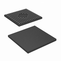
CY7C0852V-133BBCT Cypress Semiconductor Corp, CY7C0852V-133BBCT Datasheet - Page 11

CY7C0852V-133BBCT
Manufacturer Part Number
CY7C0852V-133BBCT
Description
CY7C0852V-133BBCT
Manufacturer
Cypress Semiconductor Corp
Datasheet
1.CY7C0851V-167BBC.pdf
(32 pages)
Specifications of CY7C0852V-133BBCT
Format - Memory
RAM
Memory Type
SRAM - Dual Port, Synchronous
Memory Size
4M (128K x 36)
Speed
133MHz
Interface
Parallel
Voltage - Supply
3.135 V ~ 3.465 V
Operating Temperature
0°C ~ 70°C
Package / Case
172-LFBGA
Lead Free Status / RoHS Status
Contains lead / RoHS non-compliant
Available stocks
Company
Part Number
Manufacturer
Quantity
Price
Company:
Part Number:
CY7C0852V-133BBCT
Manufacturer:
Cypress Semiconductor Corp
Quantity:
10 000
Document #: 38-06059 Rev. *I
IEEE 1149.1 Serial Boundary Scan (JTAG)
The CY7C0851V/CY7C0852V incorporates an IEEE 1149.1
serial boundary scan test access port (TAP). The TAP
controller functions in a manner that does not conflict with the
operation of other devices using 1149.1-compliant TAPs. The
TAP operates using JEDEC-standard 3.3V I/O logic levels. It
is composed of three input connections and one output
connection required by the test logic defined by the standard.
Disabling the JTAG Feature
It is possible to operate the CY7C0851V/CY7C0852V without
using the JTAG feature. To disable the TAP controller, TCK
must be tied LOW (V
and TMS are internally pulled up and may be unconnected.
They may alternatively be connected to V
resistor. TDO should be left unconnected.
Test Access Port–Test Clock (TCK)
The test clock is used only with the TAP controller. All inputs
are captured on the rising edge of TCK. All outputs are driven
from the falling edge of TCK.
Test Mode Select (TMS)
The TMS input is used to give commands to the TAP controller
and is sampled on the rising edge of TCK. It is allowable to
leave this pin unconnected if the TAP is not used. The pin is
pulled up internally, resulting in a logic HIGH level.
Notes:
12. Boundary scan is IEEE 1149.1-compatible. See “Performing a Pause/Restart” for deviation from strict 1149.1 compliance.
11. The “X” in this diagram represents the counter upper bits.
SS
Example:
Load
Counter-Mask
Register = 3F
Load
Address
Counter = 8
Max + 1
Address
Register
Max
Address
Register
) to prevent clocking of the device. TDI
Figure 2. Programmable Counter-Mask Register Operation
CNTINT
DD
H
H
L
H
through a pull-up
2
2
2
2
16
16
16
16
X
0
X
X
2
2
2
2
15
15
15
15
X
0
X
X
[12]
Masked Address
Xs
0s
Xs
Xs
Test Data-In (TDI)
The TDI pin is used to serially input information into the
registers and can be connected to the input of any of the
registers. The register between TDI and TDO is chosen by the
instruction that is loaded into the TAP instruction register. For
information on loading the instruction register, see the TAP
Controller State Diagram. TDI is internally pulled up and can
be unconnected if the TAP is unused in an application. TDI is
connected to the MSB on any register.
Test Data Out (TDO)
The TDO output pin is used to serially clock data out from the
registers. The output is active depending upon the current
state of the TAP state machine (see TAP Controller State
Diagram [FSM]). The output changes on the falling edge of
TCK. TDO is connected to the LSB of any register.
Performing a TAP Reset
A reset is performed by forcing TMS HIGH (V
edges of TCK. This reset does not affect the operation of the
CY7C0851V/CY7C0852V, and may be performed while the
device is operating. An MRST must be performed on the
CY7C0851V/CY7C0852V after power-up.
Performing a Pause/Restart
When a SHIFT-DR PAUSE-DR SHIFT-DR is performed the
scan chain will output the next bit in the chain twice. For
example, if the value expected from the chain is 1010101, the
device will output a 11010101. This extra bit will cause some
testers
CY7C0851V/CY7C0852V in a scan test. Therefore the tester
should be configured to never enter the PAUSE-DR state.
2
2
2
2
6
6
6
6
to
X
0
X
X
2
2
2
2
5
5
5
5
0 0
1 1
0 0
1 1
report
Unmasked Address
2
2
2
2
4
4
4
4
2
2
2
2
CY7C0851V/CY7C0852V
CY7C0831V/CY7C0832V
3
3
3
3
1
1
1
1
2
2
2
2
2
an
2
2
2
0
1
0
1
2
[1, 11]
2
2
2
1
1
1
1
0
1
0
1
erroneous
2
2
2
2
0
0
0
0
0
1
0
1
Mask
Register
bit-0
Address
Counter
bit-0
failure
DD
Page 11 of 32
) for five rising
for
the


