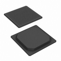
CYD36S36V18-167BGXI Cypress Semiconductor Corp, CYD36S36V18-167BGXI Datasheet - Page 10

CYD36S36V18-167BGXI
Manufacturer Part Number
CYD36S36V18-167BGXI
Description
CYD36S36V18-167BGXI
Manufacturer
Cypress Semiconductor Corp
Datasheet
1.CYD02S36V18-167BBC.pdf
(52 pages)
Specifications of CYD36S36V18-167BGXI
Format - Memory
RAM
Memory Type
SRAM - Dual Port, Synchronous
Memory Size
36M (1M x 36)
Speed
167MHz
Interface
Parallel
Voltage - Supply
1.42 V ~ 1.58 V, 1.7 V ~ 1.9 V
Operating Temperature
-40°C ~ 85°C
Package / Case
484-BGA
Lead Free Status / RoHS Status
Lead free / RoHS Compliant
Available stocks
Company
Part Number
Manufacturer
Quantity
Price
Company:
Part Number:
CYD36S36V18-167BGXI
Manufacturer:
Cypress Semiconductor Corp
Quantity:
10 000
Pin Definitions
Note
Document Number: 38-06082 Rev. *J
PORTSTD[1:0]
R/W
READY
CNT/MSK
ADS
CNTEN
CNTRST
CNTINT
WRP
RET
VREF
VDDIO
FTSEL
MRST
TMS
TDI
TRST
TCK
TDO
VSS
VCORE
VTTL
26. PORTSTD[1:0]
Left Port
L
L
L
L
L
L
L
L
L
L
L
L
L
[26]
L
and PORTSTD[1:0]
PORTSTD[1:0]
R/W
READY
CNT/MSK
ADS
CNTEN
CNTRST
CNTINT
WRP
RET
VREF
VDDIO
FTSEL
Right Port
(continued)
R
R
R
R
R
R
R
R
R
R
R
R
R
R
[26]
have internal pull-down resistors.
Port clock/Address/Control/Data/Echo clock/I/O standard select input. Assert these pins
LOW/LOW for LVTTL, LOW/HIGH for HSTL, HIGH/LOW for 2.5 V LVCMOS, and HIGH/HIGH for
1.8 V LVCMOS, respectively. These pins are driven by VTTL referenced levels.
Read/Write enable input. Assert this pin LOW to write to, or HIGH to read from the dual port
memory array.
Port DLL ready output. This signal is asserted LOW when the DLL and variable impedance
matching circuits complete calibration. This is a wired OR capable output.
Port counter/Mask select input. Counter control input.
Port counter address load strobe input. Counter control input.
Port counter enable input. Counter control input.
Port counter reset input. Counter control input.
Port counter interrupt output. This pin is asserted LOW one cycle before the unmasked portion
of the counter is incremented to all “1s”.
Port counter wrap input. When the burst counter reaches the maximum count, on the next
counter increment WRP is set LOW to load the unmasked counter bits to 0. It is set HIGH to load
the counter with the value stored in the mirror register.
Port counter retransmit input. Assert this pin LOW to reload the initial address for repeated
access to the same segment of memory.
Port external HSTL IO reference input. This pin is left DNU when HSTL is not used.
Port data IO power supply.
Port flow through mode select input. Assert this pin LOW to select flow through mode. Assert
this pin HIGH to select Pipelined mode.
Master reset input. MRST is an asynchronous input signal and affects both ports. Asserting
MRST LOW performs all of the reset functions as described in the text. A MRST operation is
required at power up. This pin is driven by a VDDIO
JTAG test mode select input. It controls the advance of JTAG TAP state machine. State
machine transitions occur on the rising edge of TCK. Operation for LVTTL or 2.5 V LVCMOS.
JTAG test data input. Data on the TDI input is shifted serially into selected registers. Operation
for LVTTL or 2.5 V LVCMOS.
JTAG reset input. Operation for LVTTL or 2.5 V LVCMOS.
JTAG test clock input. Operation for LVTTL or 2.5 V LVCMOS.
JTAG test data output. TDO transitions occur on the falling edge of TCK. TDO is normally
tri-stated except when captured data is shifted out of the JTAG TAP. Operation for LVTTL or
2.5 V LVCMOS.
Ground inputs.
Device core power supply.
LVTTL power supply.
Description
L
referenced signal.
Page 10 of 52
FullFlex
[+] Feedback


