EVAL-ADF7021-NDBEZ Analog Devices Inc, EVAL-ADF7021-NDBEZ Datasheet - Page 42
EVAL-ADF7021-NDBEZ
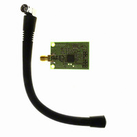
Manufacturer Part Number
EVAL-ADF7021-NDBEZ
Description
426MHz To 429 MHz, External L
Manufacturer
Analog Devices Inc
Type
Transceiver, FSKr
Datasheet
1.ADF7021-NBCPZ-RL.pdf
(64 pages)
Specifications of EVAL-ADF7021-NDBEZ
Frequency
420MHz ~ 440MHz
Lead Free Status / RoHS Status
Lead free / RoHS Compliant
For Use With/related Products
ADF7021-N
Lead Free Status / RoHS Status
Lead free / RoHS Compliant
Other names
Q5835434A


ADF7021-N
PACKET STRUCTURE AND CODING
The suggested packet structure to use with the ADF7021-N is
shown in Figure 54.
Refer to the Receiver Setup section for information on the
required preamble structure and length for the various modulation
schemes.
PROGRAMMING AFTER INITIAL POWER-UP
Table 23 lists the minimum number of writes needed to set up
the ADF7021-N in either Tx or Rx mode after CE is brought
high. Additional registers can also be written to tailor the part
PREAMBLE
Figure 54. Typical Format of a Transmit Protocol
WORD
SYNC
FIELD
ID
DATA FIELD
CRC
Rev. 0 | Page 42 of 64
to a particular application, such as setting up sync byte
detection or enabling AFC. When going from Tx to Rx or vice
versa, the user needs to toggle the Tx/Rx bit and write only to
Register 0 to alter the LO by 100 kHz.
Table 23. Minimum Register Writes Required for Tx/Rx Setup
Mode
Tx
Rx
Tx to Rx and Rx to Tx
The recommended programming sequences for transmit and
receive are shown in Figure 55 and Figure 56, respectively. The
difference in the power-up routine for a TCXO and XTAL
reference is shown in these figures.
Reg 1
Reg 1
Reg 0
Reg 3
Reg 3
Registers
Reg 0
Reg 0
Reg 2
Reg 5
Reg 4
Related parts for EVAL-ADF7021-NDBEZ
Image
Part Number
Description
Manufacturer
Datasheet
Request
R

Part Number:
Description:
±1.7g Dual-Axis IMEMS Accelerometer Evaluation Board
Manufacturer:
Analog Devices Inc
Datasheet:

Part Number:
Description:
Inertial Sensor Evaluation System
Manufacturer:
Analog Devices Inc
Datasheet:
Part Number:
Description:
Manufacturer:
Analog Devices Inc
Datasheet:
Part Number:
Description:
Manufacturer:
Analog Devices Inc
Datasheet:
Part Number:
Description:
Manufacturer:
Analog Devices Inc
Datasheet:
Part Number:
Description:
Manufacturer:
Analog Devices Inc
Datasheet:
Part Number:
Description:
Manufacturer:
Analog Devices Inc
Datasheet:
Part Number:
Description:
Manufacturer:
Analog Devices Inc
Datasheet:
Part Number:
Description:
Manufacturer:
Analog Devices Inc
Datasheet:
Part Number:
Description:
Manufacturer:
Analog Devices Inc
Datasheet:
Part Number:
Description:
Manufacturer:
Analog Devices Inc
Datasheet:
Part Number:
Description:
Manufacturer:
Analog Devices Inc
Datasheet:
Part Number:
Description:
Manufacturer:
Analog Devices Inc
Datasheet: