JM38510/10103BGA National Semiconductor, JM38510/10103BGA Datasheet
JM38510/10103BGA
Specifications of JM38510/10103BGA
Available stocks


Related parts for JM38510/10103BGA


JM38510/10103BGA Summary of contents
Page 1
... It has advantages over internally compensated amplifiers in that the frequency compensation can be tailored to the particular applica- Ordering Information NS Part Number SMD Part Number JL101ABGA JM38510/10103BGA JL101ABPA JM38510/10103BPA JL101ABHA JM38510/10103BHA JL101ABCA JM38510/10103BCA JL101ASGA ...
Page 2
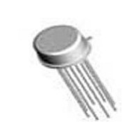
Schematic (Note 8) Connection Diagrams (Top View) Metal Can Package Note: Pin 4 connected to case. See NS Package Number H08C www.national.com See NS Package Number J08A 20129602 2 20129601 (Top View) Dual-In-Line Package 20129604 ...
Page 3
Connection Diagrams (Top View) Dual-In-Line Package See NS Package Number J14A Fast AC/DC Converter Note 1: Feedforward compensation can be used to make a fast full wave rectifier without a filter. (Continued) 20129603 3 (Top View) Ceramic Flatpack Package 20129640 ...
Page 4
Absolute Maximum Ratings Supply Voltage Differential Input Voltage Input Voltage (Note 3) Output Short Circuit Duration Operating Ambient Temp. Range T Max J Power Dissipation 25˚C (Note 4) A H-Package (Still Air) (500 LF / Min Air ...
Page 5
Quality Conformance Inspection Mil-Std-883, Method 5005 - Group A Subgroup LM101A JAN Electrical Characteristics DC Parameters The following conditions apply to all parameters, unless otherwise specified ± V ...
Page 6
LM101A JAN Electrical Characteristics DC Parameters (Continued) The following conditions apply to all parameters, unless otherwise specified ± 20V 0V 50Ω Symbol Parameters CMRR Common Mode Rejection Ratio V +V Adj ...
Page 7
LM101A JAN Electrical Characteristics DC Parameters: Drift Values The following conditions apply to all parameters, unless otherwise specified ± 20V 0V 50Ω Delta calculations performed on JAN S devices at group ...
Page 8
Typical Performance Characteristics Input Voltage Range Voltage Gain Supply Current www.national.com LM101A 20129641 20129643 20129647 8 Output Swing 20129642 Voltage Gain 20129648 ...
Page 9
Typical Performance Characteristics Maximum Power Dissipation Current Limiting Input Noise Current LM101A (Continued) 20129649 20129651 Common Mode Rejection 20129653 9 Input Current, LM101A 20129650 Input Noise Voltage 20129652 20129654 www.national.com ...
Page 10
Typical Performance Characteristics Power Supply Rejection www.national.com LM101A (Continued) Closed Loop Output 20129655 10 Impedance 20129656 ...
Page 11
Typical Performance Characteristics for Various Compensation Circuits (Note 8) Single Pole Compensation Feedforward Compensation MHz o Open Loop Frequency Response 20129608 20129616 20129613 ...
Page 12
Typical Performance Characteristics for Various Compensation Circuits (Note 8) (Continued) Large Signal Frequency Response Large Signal Frequency Response Voltage Follower Pulse Response www.national.com Large Signal Frequency 20129610 20129618 Inverter Pulse Response 20129615 12 Response 20129614 Voltage Follower Pulse Response 20129611 ...
Page 13
Typical Applications (Note 8) Variable Capacitance Multiplier Simulated Inductor Fast Inverting Amplifier with High Input Impedance 20129620 † May be zero or equal to parallel combination of ...
Page 14
Application Hints (Note 8) *Protects input † Protects output ‡ Protects output — not needed when R4 is used. www.national.com Protecting Against Gross Fault Conditions Compensating for Stray Input Capacitances or Large Feedback Resistor 20129627 Isolating Large Capacitive Loads 14 ...
Page 15
Although the LM101A is designed for trouble free operation, experience has indicated that it is wise to observe certain precautions given below to protect the devices from abnor- mal operating conditions. It might be pointed out that the advice given ...
Page 16
Typical Applications (Note 8) (Continued Note 9: Feedforward compensation can be used to make a fast full wave rectifier without a filter. www.national.com Bilateral Current Source 20129632 Fast AC/DC Converter (Note 9) ...
Page 17
Typical Applications (Note 8) (Continued R4 † *, Matching determines CMRR. Integrator with Bias Current Compensation *Adjust for zero integrator drift. Current drift typically 0.1 nA/˚C over 0˚C to +70˚C temperature range. Instrumentation Amplifier Voltage ...
Page 18
Typical Applications (Note 8) (Continued) Low Drift Sample and Hold *Polycarbonate-dielectric capacitor www.national.com Low Frequency Square Wave Generator Voltage Comparator for Driving DTL or TTL Integrated Circuits 20129638 18 20129636 20129639 ...
Page 19
Revision History Section Date Revision Section Released 01/05/06 A New Release to corporate format Originator Changes L. Lytle 1 MDS datasheets converted into one Corp. datasheet format. MJLM101A-X Rev 1A0 datasheet will be archived. 19 www.national.com ...
Page 20
Physical Dimensions www.national.com inches (millimeters) unless otherwise noted Metal Can Package (H) NS Package Number H08C Ceramic Dual-In-Line Package (J) NS Package Number J08A 20 ...
Page 21
Physical Dimensions inches (millimeters) unless otherwise noted (Continued) Ceramic Dual-In-Line Package (J) NS Package Number J14A Ceramic Flatpack Package (W) NS Package Number W10A 21 www.national.com ...
Page 22
... BANNED SUBSTANCE COMPLIANCE National Semiconductor manufactures products and uses packing materials that meet the provisions of the Customer Products Stewardship Specification (CSP-9-111C2) and the Banned Substances and Materials of Interest Specification (CSP-9-111S2) and contain no ‘‘Banned Substances’’ as defined in CSP-9-111S2. ...