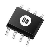
NCS2553DR2G ON Semiconductor, NCS2553DR2G Datasheet - Page 4

NCS2553DR2G
Manufacturer Part Number
NCS2553DR2G
Description
IC TRPL VIDEO AMP W/FILTER 8SOIC
Manufacturer
ON Semiconductor
Specifications of NCS2553DR2G
Applications
Filter
Number Of Circuits
3
-3db Bandwidth
8MHz
Current - Supply
23mA
Voltage - Supply, Single/dual (±)
4.75 V ~ 5.25 V
Mounting Type
Surface Mount
Package / Case
8-SOIC (0.154", 3.90mm Width)
Supply Type
Single
Minimum Operating Temperature
- 40 C
Maximum Operating Temperature
+ 85 C
Mounting Style
SMD/SMT
Supply Voltage (max)
5.25 V
Supply Voltage (min)
4.75 V
Lead Free Status / RoHS Status
Lead free / RoHS Compliant
Available stocks
Company
Part Number
Manufacturer
Quantity
Price
Company:
Part Number:
NCS2553DR2G
Manufacturer:
ON
Quantity:
5 550
Part Number:
NCS2553DR2G
Manufacturer:
ON/安森美
Quantity:
20 000
NOTE: Device will meet the specifications after thermal equilibrium has been established when mounted in a test socket or printed circuit
NOTE: Device will meet the specifications after thermal equilibrium has been established when mounted in a test socket or printed circuit
5. 100% of tested IC fit to the bandwidth tolerance.
6. Guaranteed by design and characterization.
7. SNR = 20 x log (714 mV/RMS Noise)
DC ELECTRICAL CHARACTERISTICS
coupled outputs into 150 W load, referenced to 400 kHz, unless otherwise specified)
AC ELECTRICAL CHARACTERISTICS
coupled outputs into 150 W load, referenced to 400 kHz, unless otherwise specified)
V
I
V
PSRR
A
BW
A
dG
dq
THD
X
SNR
Tpd
DGD
Symbol
Symbol
CC
VOL
CC
IN
R
talk
board with maintained transverse airflow greater than 500 lfpm. Electrical parameters are guaranteed only over the declared
operating temperature range. Functional operation of the device exceeding these conditions is not implied. Device specification limit
values are applied individually under normal operating conditions and not valid simultaneously.
Supply Voltage Range
Power Supply Current
Input Common Mode Voltage Range
Power Supply Rejection
Voltage Gain (Note 5)
Low Pass Filter Bandwidth
Stop−Band Attenuation (Rejection)
Differential Gain
Differential Phase
Total Harmonic Distortion
Channel−to−Channel Crosstalk
Signal−to−Noise Ratio
Propagation Delay
Group Delay Variation from 100 kHz to
8 MHz
Characteristics
Characteristics
(V
(V
CC
CC
= +5.0 V, T
= +5.0 V, T
http://onsemi.com
Referenced to GND if DC−Coupled
NTSC−7, 100 kHz to 4.2 MHz
A
A
V
V
Input−to−Output, 4.5 MHz
= 25°C, 0.1 mF AC coupled inputs, R
= 25°C, 0.1 mF AC coupled inputs, R
V
OUT
OUT
IN
4
DC (All Channels)
= 1 V (All Channels)
−1 dB (Note 6)
= 1.8 V
= 1.8 V
Conditions
Conditions
at 27 MHz
No Load
(Note 7)
−3 dB
PP
PP
@ 1 MHz
@ 1 MHz
GND
4.75
Min
Min
5.8
5.5
source
source
= 37.5 W, 220 mF AC
= 37.5 W,220 mF AC
Typ
−50
Typ
−60
5.0
6.0
7.2
9.0
0.3
0.6
0.4
23
45
75
60
27
Max
5.25
Max
1.4
6.2
30
nsec
MHz
MHz
Unit
Unit
mA
dB
dB
dB
dB
dB
ns
%
%
V
_


