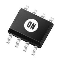
NCS2553DR2G ON Semiconductor, NCS2553DR2G Datasheet - Page 7

NCS2553DR2G
Manufacturer Part Number
NCS2553DR2G
Description
IC TRPL VIDEO AMP W/FILTER 8SOIC
Manufacturer
ON Semiconductor
Specifications of NCS2553DR2G
Applications
Filter
Number Of Circuits
3
-3db Bandwidth
8MHz
Current - Supply
23mA
Voltage - Supply, Single/dual (±)
4.75 V ~ 5.25 V
Mounting Type
Surface Mount
Package / Case
8-SOIC (0.154", 3.90mm Width)
Supply Type
Single
Minimum Operating Temperature
- 40 C
Maximum Operating Temperature
+ 85 C
Mounting Style
SMD/SMT
Supply Voltage (max)
5.25 V
Supply Voltage (min)
4.75 V
Lead Free Status / RoHS Status
Lead free / RoHS Compliant
Available stocks
Company
Part Number
Manufacturer
Quantity
Price
Company:
Part Number:
NCS2553DR2G
Manufacturer:
ON
Quantity:
5 550
Part Number:
NCS2553DR2G
Manufacturer:
ON/安森美
Quantity:
20 000
Standard Definition video applications covering the
requirements of the CVBS, S−Video, 480i/525i & 576i/625i
standards. All the 3 channels feature the same specifications
and similar behaviors guaranteed by a high channel−to−
channel crosstalk isolation (down to 60 dB at 1 MHz). Each
channel provides an internal voltage−to−voltage gain of 2
from its input to its output reducing the number of external
components usually needed in the case of some discrete
approaches (using stand−alone op amps). An internal level
shifter is employed shifting up the output voltage by adding
an offset of about 280 mV. This avoids sync pulse clipping
source coming from the DAC is AC−coupled at the input and
output. But thanks to the built−in transparent clamp and
level shifter the device can operate in different configuration
modes depending essentially on the DAC output signal level
High and Low and how it fits the input common mode
voltage of the video driver. When the configuration is
DC−Coupled at the Inputs and Outputs the 0.1 mF and
220 mF coupling capacitors are no longer used, the clamps
are in that case inactive; this configuration has the big
advantage of being relatively low cost with the use of less
external components.
The NCS2553 triple video driver has been optimized for
Figure 13 shows an example for which the external video
DAC
Y, R’, G’, B’
Pb, Pr
1V
0V
R
R
R
S
S
S
0.7V
0.1mF
0.1mF
0.1mF
0V
Figure 13. AC−Coupled Inputs and Outputs
APPLICATIONS INFORMATION
IN1
IN2
IN3
800k
800k
800k
http://onsemi.com
280mV
280mV
280mV
LS
LS
LS
8MHz
8MHz
8MHz
7
2.28V
0.28V
and allows DC−coupled output to the 150 W video load. In
addition, the NCS2553 integrates a 6
filter per channel with a 3 dB frequency bandwidth of 8
MHz. This allows rejecting out the aliases or unwanted
over−sampling effects produced by the video DAC.
Similarly, in the case of DVD recorders using ADC, this
anti−aliasing filter (reconstruction filter) will avoid picture
quality issues and will help to filter out parasitic signals
caused by EMI interference.
channel to support AC−coupled mode of operation. The
clamp is active when the input signal goes below 0 V.
amplitude goes over the range 0 to 1.4 V or if the video
source requires such a coupling. In some circumstances it
may be necessary to auto−bias signals by the addition of a
pull−up and pull−down resistor or only pull−up resistor
(Typical 7.5 MW combined with the internal 800 kW
pull−down) making the clamp inactive.
of eliminating DC ground loop with the drawback of making
the device more sensitive to video line or field tilt issues in
the case of a too low output coupling capacitor. In some
cases it may be necessary to increase the nominal 220 mF
capacitor value.
A built−in diode−like clamp is used in the chip for each
The input is AC−coupled if for example the input−signal
The output AC−coupling configuration has the advantage
6db
6db
6db
OUT1
OUT2
OUT3
1.68V
0.28V
220mF
220mF
220mF
75W
75W
75W
0.7V
1V
PP
Z
Z
Z
PP
O
O
O
= 75W
= 75W
= 75W
th
order Butterworth
75W
75W
75W


