RDK-251 Power Integrations, RDK-251 Datasheet - Page 11
RDK-251
Manufacturer Part Number
RDK-251
Description
KIT REF DESIGN FOR LNK457D
Manufacturer
Power Integrations
Series
LinkSwitch®-PLr
Datasheet
1.RDK-251.pdf
(60 pages)
Specifications of RDK-251
Current - Output / Channel
350mA
Outputs And Type
1, Isolated
Voltage - Output
12 ~ 18 V
Features
Dimmable
Voltage - Input
90 ~ 265VAC
Utilized Ic / Part
LNK457D
Output Voltage
12 V
Input / Supply Voltage (max)
265 VAC
Input / Supply Voltage (min)
90 VAC
Duty Cycle (max)
39.9 %
Mounting Style
Through Hole
Output Current
350 mA
Output Power
5 W
Lead Free Status / RoHS Status
Lead free / RoHS Compliant
Other names
596-1345
Available stocks
Company
Part Number
Manufacturer
Quantity
Price
Company:

Part Number:
RDK-251
Manufacturer:
Power Integrations
Quantity:
135


15-Feb-11
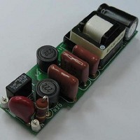
RDR-251 – 5 W, PFC, Dimmable LED Power Supply
4.5 LinkSwitch-PL Primary
The LNK457DG device (U1) incorporates the power switching device, oscillator, output
constant current control, start-up, and protection functions. The integrated 725 V
MOSFET provides extended voltage margin and ensures high reliability even during line
surge events. The device is powered from the BYPASS pin via the decoupling capacitor
C9. At start-up, C9 is charged by U1 from an internal current source via the DRAIN pin
and then during normal operation it is supplied by the output via R15 and D4.
The rectified and filtered input voltage is applied to one end of the primary winding of T1.
The other side of the transformer’s primary winding is driven by the integrated MOSFET
in U1. The leakage inductance drain voltage spike is limited by an RCD-R clamp
consisting of D2, R13, R12, and C7.
Diode D6 is used to protect the IC from negative ringing (drain voltage ringing below
source voltage) when the MOSFET is off due to the reflected output voltage exceeding
the DC bus voltage, the result of minimal input capacitance to give high power factor.
4.6 Output Rectification
The secondary of the transformer is rectified by D5 and filtered by C11. A Schottky
barrier type was selected for higher efficiency. As C11 provides energy storage during
AC zero crossings its value determines the magnitude of the line frequency output ripple
(2 x f
due to full wave rectification). The value may therefore be adjusted based on the
L
desired output ripple. For the 680 F value shown the output ripple is 50% of I
.
O
Resistor R17 and C10 damp high frequency ringing and improve conducted and radiated
EMI.
4.7 Output Feedback
The CC mode set-point is determined by the voltage drop that appears across R18 which
is then fed to the FB pin of U1. Output overvoltage protection is provided by VR2 and
R14 (the effect of R14 on the current sense signal in negligible and can be ignored).
Power Integrations
Tel: +1 408 414 9200 Fax: +1 408 414 9201
Page 11 of 60
www.powerint.com
Related parts for RDK-251
Image
Part Number
Description
Manufacturer
Datasheet
Request
R

Part Number:
Description:
KIT REF DESIGN TOP HX FOR TOP258
Manufacturer:
Power Integrations
Datasheet:

Part Number:
Description:
KIT REF DESIGN LINKSWITCH 2
Manufacturer:
Power Integrations
Datasheet:

Part Number:
Description:
KIT REF DESIGN 1.2W PS TN FAMILY
Manufacturer:
Power Integrations
Datasheet:

Part Number:
Description:
KIT REF DESIGN 36-72W MOTOR DRVR
Manufacturer:
Power Integrations
Datasheet:

Part Number:
Description:
REFERENCE DESIGN LINKSWITCH-PH
Manufacturer:
Power Integrations
Datasheet:

Part Number:
Description:
Specifications: Manufacturer: Power Integrations ; Output Voltage: 380 VDC ; Input / Supply Voltage (Max): 264 VAC ; Input / Supply Voltage (Min): 90 VAC ; Mounting Style: Through Hole ; Output Current: 0.913 A ; Output Power: 347 W
Manufacturer:
Power Integrations, Inc.

Part Number:
Description:
Power Management Modules & Development Tools TOPSwitch-JX REF. DESIGN KIT
Manufacturer:
Power Integrations
Datasheet:
Part Number:
Description:
Power Management IC Development Tools REF DESIGN RDR-292 PFF LED STREET LIGHT
Manufacturer:
Power Integrations

Part Number:
Description:
KIT REF DESIGN FOR LNK403EG
Manufacturer:
Power Integrations
Datasheet:

Part Number:
Description:
KIT REF DESIGN FOR LNK406EG
Manufacturer:
Power Integrations
Datasheet:
Part Number:
Description:
KIT REF DESIGN 36-72W MOTOR DRVR
Manufacturer:
Power Integrations
Datasheet:
Part Number:
Description:
REFERENCE DESIGN LINKSWITCH-PH
Manufacturer:
Power Integrations
Datasheet:
Part Number:
Description:
Specifications: Manufacturer: Power Integrations ; Output Voltage: 380 VDC ; Input / Supply Voltage (Max): 264 VAC ; Input / Supply Voltage (Min): 90 VAC ; Mounting Style: Through Hole ; Output Current: 0.913 A ; Output Power: 347 W
Manufacturer:
Power Integrations, Inc.
Part Number:
Description:
Specifications: Family: Eval Boards - DC/DC & AC/DC (Off-Line) SMPS ; Series: HiperLCS™ ; Main Purpose: DC/DC, Step Down ; Outputs and Type: 1, Isolated ; Power - Output: 150W ; Voltage - Output: 24V ; Current - Output: 6.25A ; Voltage - Input:
Manufacturer:
Power Integrations, Inc.
Datasheet: