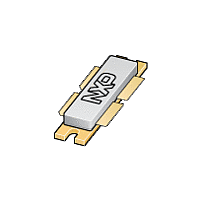
BLF6G20-230PRN NXP Semiconductors, BLF6G20-230PRN Datasheet - Page 6

BLF6G20-230PRN
Manufacturer Part Number
BLF6G20-230PRN
Description
RF MOSFET Small Signal 230W, 1800-2000MHz
Manufacturer
NXP Semiconductors
Datasheet
1.BLF6G20-230PRN.pdf
(13 pages)
Specifications of BLF6G20-230PRN
Configuration
Dual Common Source
Transistor Polarity
N-Channel
Resistance Drain-source Rds (on)
0.165 Ohms
Drain-source Breakdown Voltage
65 V
Gate-source Breakdown Voltage
13 V
Maximum Operating Temperature
+ 225 C
Mounting Style
SMD/SMT
Minimum Operating Temperature
- 65 C
Package / Case
SOT502B
Lead Free Status / RoHS Status
Lead free / RoHS Compliant
Other names
934063293112
Available stocks
Company
Part Number
Manufacturer
Quantity
Price
Company:
Part Number:
BLF6G20-230PRN
Manufacturer:
NXP
Quantity:
1 000
Company:
Part Number:
BLF6G20-230PRN
Manufacturer:
NXP
Quantity:
5 000
NXP Semiconductors
BLF6G20-230PRN_20S-230PRN_2
Product data sheet
Fig 2.
(dB)
G
p
19
17
15
13
11
0
V
efficiency as functions of load power; typical
values
2-carrier W-CDMA power gain and drain
DS
= 28 V; I
7.2.2 2-carrier W-CDMA
G
η
D
p
20
Dq
= 2000 mA.
Fig 4.
40
V
2-carrier W-CDMA peak output power and output peak-to-average ratio as
function of load power; typical values
DS
= 28 V; I
60
All information provided in this document is subject to legal disclaimers.
P
001aal413
L
(W)
Dq
P
(W)
Rev. 02 — 9 February 2010
L(M)
= 2000 mA.
80
400
300
200
100
40
30
20
10
0
0
(%)
η
0
D
20
P
PAR
L(M)
Fig 3.
APCR
(dBc)
(1) f = 5 MHz low
(2) f = 5 MHz high
(3) f = 10 MHz low
(4) f = 10 MHz high
−20
−40
−60
−80
40
0
V
2-carrier W-CDMA adjacent channel power
ratio as function of load power; typical values
DS
BLF6G20(S)-230PRN
(1)
(3)
= 28 V; I
60
(2)
(4)
20
Dq
80
= 2000 mA.
001aal415
P
40
L
(W)
100
Power LDMOS transistor
9
7
5
3
1
60
PAR
(dB)
© NXP B.V. 2010. All rights reserved.
80
001aal414
P
L
(W)
100
6 of 13


