BAV99,215 NXP Semiconductors, BAV99,215 Datasheet - Page 6
BAV99,215
Manufacturer Part Number
BAV99,215
Description
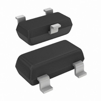
DIODE SW DBL 75V 215MA HS SOT23
Manufacturer
NXP Semiconductors
Specifications of BAV99,215
Package / Case
SOT-23-3, TO-236-3, Micro3™, SSD3, SST3
Voltage - Forward (vf) (max) @ If
1.25V @ 150mA
Current - Reverse Leakage @ Vr
500nA @ 80V
Current - Average Rectified (io) (per Diode)
215mA (DC)
Voltage - Dc Reverse (vr) (max)
100V
Reverse Recovery Time (trr)
4ns
Diode Type
Standard
Speed
Fast Recovery =< 500ns, > 200mA (Io)
Diode Configuration
1 Pair Series Connection
Mounting Type
Surface Mount
Product
Switching Diodes
Peak Reverse Voltage
100 V
Forward Continuous Current
0.215 A
Max Surge Current
4 A
Configuration
Dual Series
Recovery Time
4 ns
Forward Voltage Drop
1.25 V
Maximum Reverse Leakage Current
0.5 uA
Operating Temperature Range
+ 150 C
Maximum Operating Temperature
+ 150 C
Minimum Operating Temperature
- 65 C
Mounting Style
SMD/SMT
Rectifier Type
Switching Diode
Peak Rep Rev Volt
100V
Avg. Forward Curr (max)
0.215A
Rev Curr
0.5uA
Peak Non-repetitive Surge Current (max)
4A
Forward Voltage
1.25V
Operating Temp Range
-65C to 150C
Package Type
TO-236AB
Rev Recov Time
4ns
Operating Temperature Classification
Military
Mounting
Surface Mount
Pin Count
3
Lead Free Status / RoHS Status
Lead free / RoHS Compliant
Lead Free Status / RoHS Status
Lead free / RoHS Compliant, Lead free / RoHS Compliant
Other names
568-1624-2
933215370215
BAV99 T/R
933215370215
BAV99 T/R
Available stocks
Company
Part Number
Manufacturer
Quantity
Price
Company:

Part Number:
BAV99,215
Manufacturer:
NXP Semiconductors
Quantity:
4 800
Part Number:
BAV99,215
Manufacturer:
NXP/恩智浦
Quantity:
20 000


NXP Semiconductors
8. Test information
BAV99_SER
Product data sheet
Fig 5.
Fig 6.
R
V = V
(1) I
S
R
S
= 50 Ω
Input signal: reverse pulse rise time t
Oscilloscope: rise time t
Input signal: forward pulse rise time t
Reverse recovery time test circuit and waveforms
Forward recovery voltage test circuit and waveforms
R
R
= 50
I
+ I
= 1 mA
F
Ω
×
R
S
1 kΩ
8.1 Quality information
D.U.T.
This product has been qualified in accordance with the Automotive Electronics Council
(AEC) standard Q101 - Stress test qualification for discrete semiconductors, and is
suitable for use in automotive applications.
450 Ω
I
F
r
D.U.T.
= 0.35 ns
OSCILLOSCOPE
R
i
= 50 Ω
All information provided in this document is subject to legal disclaimers.
OSCILLOSCOPE
r
r
mga881
= 0.6 ns; reverse voltage pulse duration t
= 20 ns; forward current pulse duration t
SAMPLING
R
i
= 50
Rev. 8 — 18 November 2010
Ω
I
V
R
10 %
t
r
t
10 %
r
90 %
input signal
90 %
input signal
t
p
t
p
p
p
≥ 100 ns; duty cycle δ ≤ 0.005
= 100 ns; duty cycle δ = 0.05
t
High-speed switching diodes
t
BAV99 series
V
+ I
F
V FR
output signal
output signal
© NXP B.V. 2010. All rights reserved.
t rr
mga882
(1)
t
6 of 14
t
Related parts for BAV99,215
Image
Part Number
Description
Manufacturer
Datasheet
Request
R

Part Number:
Description:
DIODE DUAL 100V 215MA H-S SOT-23
Manufacturer:
NXP Semiconductors
Datasheet:

Part Number:
Description:
DIODE SWITCHING DUAL SOT-23
Manufacturer:
NXP Semiconductors
Datasheet:

Part Number:
Description:
SWITCHING DIODE, 100V 215mA, SOT-23
Manufacturer:
NXP Semiconductors
Datasheet:
Part Number:
Description:
Diodes - General Purpose, Power, Switching SWTCH 100V 215mA
Manufacturer:
NXP Semiconductors

Part Number:
Description:
DIODE SW SERIES 80V SOT-323
Manufacturer:
Infineon Technologies

Part Number:
Description:
DIODE SW DUAL SERIES 80V SOT-363
Manufacturer:
Infineon Technologies
Datasheet:

Part Number:
Description:
DIODE ARRAY 80V 200MA SOT-23
Manufacturer:
Infineon Technologies
Part Number:
Description:
DIODE SWITCHING CC SOT-323
Manufacturer:
Infineon Technologies
Part Number:
Description:
DIODE ARRAY 80V 200MA SOT323
Manufacturer:
Infineon Technologies
Part Number:
Description:
DIODE ARRAY 80V 200MA SOT323
Manufacturer:
Infineon Technologies
Part Number:
Description:
DIODE SWITCHING CC SOT-323
Manufacturer:
Infineon Technologies
Part Number:
Description:
DIODE SWITCHING SERIES SOT-323
Manufacturer:
Infineon Technologies