MBRS2H100T3G ON Semiconductor, MBRS2H100T3G Datasheet
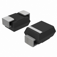
DIODE SCHOTTKY 2A 100V SMB

MBRS2H100T3G

Manufacturer Part Number
MBRS2H100T3G
Description
DIODE SCHOTTKY 2A 100V SMB
Manufacturer
ON Semiconductor
Datasheet

Specifications of MBRS2H100T3G

Voltage - Forward (vf) (max) @ If
790mV @ 2A
Voltage - Dc Reverse (vr) (max)
100V
Current - Average Rectified (io)
2A
Current - Reverse Leakage @ Vr
8µA @ 100V
Diode Type
Schottky
Speed
Fast Recovery =< 500ns, > 200mA (Io)
Mounting Type
Surface Mount
Package / Case
DO-214AA, SMB
Product
Schottky Diodes
Peak Reverse Voltage
100 V
Forward Continuous Current
2 A
Max Surge Current
130 A
Configuration
Single
Forward Voltage Drop
0.79 V
Maximum Reverse Leakage Current
8 uA
Operating Temperature Range
- 65 C to + 175 C
Mounting Style
SMD/SMT
Lead Free Status / RoHS Status
Lead free / RoHS Compliant
Reverse Recovery Time (trr)
-
Capacitance @ Vr, F
-
Lead Free Status / Rohs Status
Lead free / RoHS Compliant
Other names
MBRS2H100T3G
MBRS2H100T3GOSTR

Available stocks

Company
Part Number
Manufacturer
Quantity
Price
Part Number:
MBRS2H100T3G
Manufacturer:
ON
Quantity:
45 000
Part Number:
MBRS2H100T3G
Manufacturer:
ST
0
Part Number:
MBRS2H100T3G
Manufacturer:
ON/安森美
Quantity:
20 000
Part Number:
MBRS2H100T3G
Manufacturer:
ON
Quantity:
9 836
Part Number:
MBRS2H100T3G
Manufacturer:
ON
Quantity:
11 700
Part Number:
MBRS2H100T3G
0
Company:
Part Number:
MBRS2H100T3G
Quantity:
17 500
Company:
Part Number:
MBRS2H100T3G
Quantity:
75
Company:
Part Number:
MBRS2H100T3G
Quantity:
30 000
MBRS2H100T3G,
MBRA2H100T3G
Surface Mount
Schottky Power Rectifier
SMA/SMB Power Surface Mount Package
metal−to−silicon power rectifier. Features epitaxial construction with
oxide passivation and metal overlay contact. Ideally suited for low
voltage, high frequency switching power supplies; free wheeling
diodes and polarity protection diodes.
Features
Mechanical Characteristics
© Semiconductor Components Industries, LLC, 2009
March, 2009 − Rev. 5
This device employs the Schottky Barrier principle in a
260°C Max. for 10 Seconds
Leads are Readily Solderable
Compact Package with J−Bend Leads Ideal for Automated Handling
Highly Stable Oxide Passivated Junction
Guard−Ring for Overvoltage Protection
Low Forward Voltage Drop
This is a Pb−Free Device
Case: Molded Epoxy
Epoxy Meets UL 94 V−0 @ 0.125 in
Weight: 70 mg (SMA), 95 mg (SMB) (Approximately)
Cathode Polarity Band
Lead and Mounting Surface Temperature for Soldering Purposes:
Finish: All External Surfaces Corrosion Resistant and Terminal
ESD Ratings: Machine Model = C, Human Body Model = 3B
Device Meets MSL1 Requirements
1
†For information on tape and reel specifications,
MBRA2H100T3G
MBRS2H100T3G
including part orientation and tape sizes, please
refer to our Tape and Reel Packaging Specifications
Brochure, BRD8011/D.
A210
B210
A
Y
WW
G
(Note: Microdot may be in either location)
2.0 AMPERES, 100 VOLTS
Device
SCHOTTKY BARRIER
ORDERING INFORMATION
= MBRA2H100T3G
= MBRS2H100T3G
= Assembly Location
= Year
= Work Week
= Pb−Free Package
http://onsemi.com
CASE 403D
CASE 403A
PLASTIC
PLASTIC
RECTIFIER
SMA
SMB
(Pb−Free)
(Pb−Free)
Package
SMA
SMB
Publication Order Number:
5000 / Tape & Reel
2500 / Tape & Reel
DIAGRAMS
MARKING
MBRS2H100/D
Shipping
AYWW
AYWW
A210G
B210G
G
G

Related parts for MBRS2H100T3G

MBRS2H100T3G Summary of contents

Page 1

... March, 2009 − Rev. 5 http://onsemi.com SCHOTTKY BARRIER RECTIFIER 2.0 AMPERES, 100 VOLTS SMA CASE 403D PLASTIC SMB CASE 403A PLASTIC A210 = MBRA2H100T3G B210 = MBRS2H100T3G A = Assembly Location Y = Year WW = Work Week G = Pb−Free Package (Note: Microdot may be in either location) ORDERING INFORMATION Device Package MBRA2H100T3G SMA (Pb− ...

Page 2

MAXIMUM RATINGS Peak Repetitive Reverse Voltage Working Peak Reverse Voltage DC Blocking Voltage Average Rectified Forward Current (T = 150°C) L Non−Repetitive Peak Surge Current (Surge Applied at Rated Load Conditions Halfwave, Single Phase, 60 Hz) Storage Temperature Range Operating ...

Page 3

V , INSTANTANEOUS FORWARD VOLTAGE (V) F Figure 1. Typical Forward Voltage 10 150°C 1 125°C 0.1 0.01 0.001 25°C 0.0001 0.00001 ...

Page 4

V , REVERSE VOLTAGE (V) R Figure 5. Typical Capacitance 4.0 dc 3.0 dc 2.0 Square Wave 1 ...

Page 5

CYCLE) 100 20% 10% 5.0% 10 2.0% 1.0% 1.0 0.1 SINGLE PULSE 0.01 0.000001 0.00001 0.0001 Figure 10. Thermal Response, Junction−to−Ambient (min pad) − MBRS2H100 100 50% (DUTY CYCLE) 20% 10% 10 5.0% 2.0% 1.0 1.0% 0.1 ...

Page 6

Power Based 25°C A 2.0 1.5 1.0 0 100 200 300 400 COPPER AREA (sq mm) Figure 13 Junction−to−Ambient (URS copper area) D http://onsemi.com 6 2.0 oz 1.0 oz 500 600 700 ...

Page 7

... D POLARITY INDICATOR OPTIONAL AS NEEDED (SEE STYLES *For additional information on our Pb−Free strategy and soldering details, please download the ON Semiconductor Soldering and Mounting Techniques Reference Manual, SOLDERRM/D. PACKAGE DIMENSIONS SMA CASE 403D−02 ISSUE F NOTES: 1. DIMENSIONING AND TOLERANCING PER ANSI Y14.5M, 1982. ...

Page 8

... Pb−Free strategy and soldering details, please download the ON Semiconductor Soldering and Mounting Techniques Reference Manual, SOLDERRM/D. ON Semiconductor and are registered trademarks of Semiconductor Components Industries, LLC (SCILLC). SCILLC reserves the right to make changes without further notice to any products herein ...

Related keywords