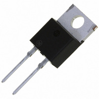
MUR2020RG ON Semiconductor, MUR2020RG Datasheet - Page 4

MUR2020RG
Manufacturer Part Number
MUR2020RG
Description
DIODE ULT FAST 20A 200V TO-220AC
Manufacturer
ON Semiconductor
Series
SWITCHMODE™r
Specifications of MUR2020RG
Voltage - Forward (vf) (max) @ If
1.1V @ 20A
Voltage - Dc Reverse (vr) (max)
200V
Current - Average Rectified (io)
20A
Current - Reverse Leakage @ Vr
50µA @ 200V
Diode Type
Standard
Speed
Fast Recovery =< 500ns, > 200mA (Io)
Reverse Recovery Time (trr)
95ns
Mounting Type
Through Hole
Package / Case
TO-220-2, TO-220AC
Product
Ultra Fast Recovery Rectifier
Configuration
Single
Reverse Voltage
200 V
Forward Voltage Drop
1.1 V
Recovery Time
95 ns
Forward Continuous Current
20 A
Max Surge Current
250 A
Reverse Current Ir
50 uA
Mounting Style
Through Hole
Maximum Operating Temperature
+ 175 C
Minimum Operating Temperature
- 65 C
Current, Forward
20 A
Current, Reverse
0.225 mA
Current, Surge
250 A
Package Type
TO-220
Primary Type
Rectifier
Resistance, Thermal, Junction To Case
2 °C/W
Speed, Switching
Ultrafast
Temperature, Junction, Maximum
+175 °C
Temperature, Operating
-65 to +175 °C
Time, Recovery
95 ns
Voltage, Forward
0.97 V
Voltage, Reverse
200 V
Lead Free Status / RoHS Status
Lead free / RoHS Compliant
Capacitance @ Vr, F
-
Lead Free Status / Rohs Status
Lead free / RoHS Compliant
Other names
MUR2020RG
MUR2020RGOS
MUR2020RGOS
Available stocks
Company
Part Number
Manufacturer
Quantity
Price
Company:
Part Number:
MUR2020RG
Manufacturer:
ON Semiconductor
Quantity:
1 931
Company:
Part Number:
MUR2020RG
Manufacturer:
ON
Quantity:
12 500
PUBLICATION ORDERING INFORMATION
SWITCHMODE is a trademark of Semiconductor Components Industries, LLC.
LITERATURE FULFILLMENT:
Literature Distribution Center for ON Semiconductor
P.O. Box 5163, Denver, Colorado 80217 USA
Phone: 303−675−2175 or 800−344−3860 Toll Free USA/Canada
Fax: 303−675−2176 or 800−344−3867 Toll Free USA/Canada
Email: orderlit@onsemi.com
ON Semiconductor and
to any products herein. SCILLC makes no warranty, representation or guarantee regarding the suitability of its products for any particular purpose, nor does SCILLC assume any liability
arising out of the application or use of any product or circuit, and specifically disclaims any and all liability, including without limitation special, consequential or incidental damages.
“Typical” parameters which may be provided in SCILLC data sheets and/or specifications can and do vary in different applications and actual performance may vary over time. All
operating parameters, including “Typicals” must be validated for each customer application by customer’s technical experts. SCILLC does not convey any license under its patent rights
nor the rights of others. SCILLC products are not designed, intended, or authorized for use as components in systems intended for surgical implant into the body, or other applications
intended to support or sustain life, or for any other application in which the failure of the SCILLC product could create a situation where personal injury or death may occur. Should
Buyer purchase or use SCILLC products for any such unintended or unauthorized application, Buyer shall indemnify and hold SCILLC and its officers, employees, subsidiaries, affiliates,
and distributors harmless against all claims, costs, damages, and expenses, and reasonable attorney fees arising out of, directly or indirectly, any claim of personal injury or death
associated with such unintended or unauthorized use, even if such claim alleges that SCILLC was negligent regarding the design or manufacture of the part. SCILLC is an Equal
Opportunity/Affirmative Action Employer. This literature is subject to all applicable copyright laws and is not for resale in any manner.
0.001
0.0000001
0.01
0.1
10
Q
1
H
L
D = 0.5
0.05
0.1
0.1
1
Single Pulse
G
B
0.000001
4
3
D
are registered trademarks of Semiconductor Components Industries, LLC (SCILLC). SCILLC reserves the right to make changes without further notice
A
K
F
0.00001
U
T
J
R
C
0.0001
N. American Technical Support: 800−282−9855 Toll Free
Europe, Middle East and Africa Technical Support:
Japan Customer Focus Center
PACKAGE DIMENSIONS
USA/Canada
Phone: 421 33 790 2910
Phone: 81−3−5773−3850
TO−220 TWO−LEAD
S
Figure 9. Thermal Response
http://onsemi.com
CASE 221B−04
MUR2020R
ISSUE D
0.001
4
t, TIME (s)
P
DUTY CYCLE, D = t
(pk)
0.01
t
1
t
2
NOTES:
1. DIMENSIONING AND TOLERANCING PER ANSI
2. CONTROLLING DIMENSION: INCH.
0.1
Y14.5M, 1982.
STYLE 2:
DIM
A
B
C
D
G
H
K
Q
R
S
U
F
J
L
T
1
PIN 1. ANODE
/t
2
2. N/A
3. CATHODE
4. ANODE
D CURVES APPLY FOR POWER
PULSE TRAIN SHOWN
READ TIME AT T
0.595
0.380
0.160
0.025
0.142
0.190
0.018
0.500
0.045
0.100
0.080
0.045
0.235
0.000
ON Semiconductor Website: www.onsemi.com
Order Literature: http://www.onsemi.com/orderlit
For additional information, please contact your local
Sales Representative
0.110
MIN
INCHES
T
J(pk)
0.620
0.405
0.190
0.035
0.147
0.210
0.130
0.025
0.562
0.060
0.120
0.055
0.255
0.050
0.110
MAX
Z
qJC(t)
1
− T
12.70
0.000
15.11
MILLIMETERS
C
MIN
9.65
4.06
0.64
3.61
4.83
2.79
0.46
1.14
2.54
2.04
1.14
5.97
= r(t) R
= P
1
(pk)
MAX
15.75
10.29
14.27
4.82
0.89
3.73
5.33
3.30
0.64
1.52
3.04
2.79
1.39
6.48
1.27
qJC
Z
MUR2020R/D
10
qJC(t)
100


