SL12-E3/61T Vishay, SL12-E3/61T Datasheet
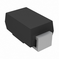
DIODE SCHOTTKY 1A 20V SMA

SL12-E3/61T

Manufacturer Part Number
SL12-E3/61T
Description
DIODE SCHOTTKY 1A 20V SMA
Manufacturer
Vishay
Datasheet

Specifications of SL12-E3/61T

Diode Type
Schottky
Voltage - Forward (vf) (max) @ If
445mV @ 1A
Voltage - Dc Reverse (vr) (max)
20V
Current - Average Rectified (io)
1.5A
Current - Reverse Leakage @ Vr
200µA @ 20V
Speed
Fast Recovery =< 500ns, > 200mA (Io)
Mounting Type
Surface Mount
Package / Case
DO-214AC, SMA
Product
Schottky Diodes
Peak Reverse Voltage
20 V
Forward Continuous Current
1.5 A
Max Surge Current
50 A
Configuration
Single
Forward Voltage Drop
0.445 V @ 1 A
Maximum Reverse Leakage Current
200 uA
Operating Temperature Range
- 55 C to + 125 C
Mounting Style
SMD/SMT
Repetitive Reverse Voltage Vrrm Max
20V
Forward Current If(av)
1.5A
Forward Voltage Vf Max
340mV
Forward Surge Current Ifsm Max
50A
Lead Free Status / RoHS Status
Lead free / RoHS Compliant
Reverse Recovery Time (trr)
-
Capacitance @ Vr, F
-
Lead Free Status / Rohs Status
Lead free / RoHS Compliant

Available stocks

Company
Part Number
Manufacturer
Quantity
Price
Part Number:
SL12-E3/61T
Manufacturer:
VISHAY/威世
Quantity:
20 000
Company:
Part Number:
SL12-E3/61T
Quantity:
70 000
Company:
Part Number:
SL12-E3/61T
Quantity:
473 400
Document Number: 88740
Revision: 22-Jan-08
PRIMARY CHARACTERISTICS
MAXIMUM RATINGS (T
PARAMETER
Device marking code
Maximum repetitive peak reverse voltage
Maximum RMS voltage
Maximum DC blocking voltage
Maximum average forward rectified current at T
Peak forward surge current 8.3 ms single half sine-wave
superimposed on rated load
Voltage rate of change (rated V
Operating junction temperature range
Storage temperature range
T
V
I
J
I
F(AV)
FSM
RRM
V
max.
F
DO-214AC (SMA)
Low V
PDD-Americas@vishay.com, PDD-Asia@vishay.com, PDD-Europe@vishay.com
For technical questions within your region, please contact one of the following:
R
)
A
= 25 °C unless otherwise noted)
F
Surface Mount Schottky Rectifier
20 V, 30 V
125 °C
0.34 V
1.5 A
50 A
L
= 105 °C (Fig. 1)
SYMBOL
V
V
I
dV/dt
T
I
V
F(AV)
FSM
RRM
RMS
T
STG
FEATURES
TYPICAL APPLICATIONS
For use in low voltage, high frequency inverters,
freewheeling,
protection applications.
MECHANICAL DATA
Case: DO-214AC (SMA)
Epoxy meets UL 94V-0 flammability rating
Terminals: Matte tin plated leads, solderable per
J-STD-002 and JESD22-B102
E3 suffix for consumer grade, meets JESD 201 class
1A whisker test, HE3 suffix for high reliability grade
(AEC Q101 qualified), meets JESD 201 class 2
whisker test
Polarity: Color band denotes the cathode end
DC
• Low profile package
• Ideal for automated placement
• Guardring for overvoltage protection
• Low power losses, high efficiency
• Very low forward voltage drop
• High surge capability
• Meets MSL level 1, per J-STD-020, LF maximum
• Solder dip 260 °C, 40 s
• Component in accordance to RoHS 2002/95/EC
J
peak of 260 °C
and WEEE 2002/96/EC
Vishay General Semiconductor
SL12
SL2
20
14
20
dc-to-dc
- 55 to + 125
- 55 to + 150
10 000
1.5
50
converters,
SL13
SL3
30
21
30
SL12 & SL13
and
www.vishay.com
UNIT
V/µs
°C
°C
polarity
V
V
V
A
A
1

Related parts for SL12-E3/61T

SL12-E3/61T Summary of contents

Page 1

... Q101 qualified), meets JESD 201 class 2 whisker test Polarity: Color band denotes the cathode end SYMBOL V RRM V RMS 105 °C (Fig F(AV) I FSM dV/ STG SL12 & SL13 Vishay General Semiconductor dc-to-dc converters, and SL12 SL13 SL2 SL3 1 000 - 125 - 150 www.vishay.com ...

Page 2

... SL12 & SL13 Vishay General Semiconductor ELECTRICAL CHARACTERISTICS (T PARAMETER Maximum instantaneous forward voltage at Maximum DC reverse current (1) at rated DC blocking voltage Note: (1) Pulse test: 300 µs pulse width duty cycle THERMAL CHARACTERISTICS (T PARAMETER (1) Maximum thermal resistance Note: (1) P.C.B. mounted on 0.2 x 0.2" (5.0 x 5.0 mm) copper pad areas ...

Page 3

... MIN. 0.110 (2.79) 0.100 (2.54) 0.177 (4.50) 0.157 (3.99) 0.060 (1.52) 0.012 (0.305) 0.006 (0.152) 0.008 (0.203) 0 (0) 0.208 (5.28) 0.194 (4.93) SL12 & SL13 Vishay General Semiconductor ° 1.0 MHz mVp-p sig 1 10 Reverse Voltage (V) Figure 5. Typical Junction Capacitance Mounting Pad Layout 0 ...

Page 4

... Vishay product could result in personal injury or death. Customers using or selling Vishay products not expressly indicated for use in such applications their own risk and agree to fully indemnify and hold Vishay and its distributors harmless from and against any and all claims, liabilities, expenses and damages arising or resulting in connection with such use or sale, including attorneys fees, even if such claim alleges that Vishay or its distributor was negligent regarding the design or manufacture of the part ...

Related keywords