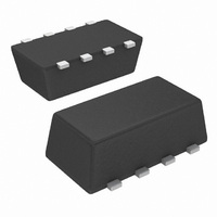
SI5511DC-T1-E3 Vishay, SI5511DC-T1-E3 Datasheet

SI5511DC-T1-E3
Specifications of SI5511DC-T1-E3
Available stocks
Related parts for SI5511DC-T1-E3
SI5511DC-T1-E3 Summary of contents
Page 1
... Bottom View Ordering Information: Si5511DC -T1-E3 (Lead (Pb)-free) Si5511DC-T1-GE3 (Lead (Pb)-free and Halogen-free) ABSOLUTE MAXIMUM RATINGS T Parameter Drain-Source Voltage Gate-Source Voltage Continuous Drain Current (T = 150 °C) J Pulsed Drain Current Source Drain Current Diode Current Maximum Power Dissipation Operating Junction and Storage Temperature Range ...
Page 2
... Si5511DC Vishay Siliconix SPECIFICATIONS °C, unless otherwise noted J Parameter Static Drain-Source Breakdown Voltage V Temperature Coefficient DS V Temperature Coefficient GS(th) Gate Threshold Voltage Gate-Body Leakage Zero Gate Voltage Drain Current b On-State Drain Current b Drain-Source On-State Resistance b Forward Transconductance a Dynamic Input Capacitance Output Capacitance ...
Page 3
... ≅ GEN ° 2 1 N-Channel 2.4 A, dI/dt = 100 A/µ P-Channel 1.5 A, dI/ 100 A/µ Si5511DC Vishay Siliconix a Min. Typ. Max Ω P-Ch 78 117 N- P- Ω N-Ch 2.6 P-Ch - 2.6 N- N-Ch 0.8 1.2 P-Ch - 0.8 - 1.2 N-Ch 11 ...
Page 4
... Si5511DC Vishay Siliconix N-CHANNEL TYPICAL CHARACTERISTICS 25 °C, unless otherwise noted thru 0.0 0.6 1 Drain-to-Source Voltage (V) DS Output Characteristics 0.20 0. 0.08 0.04 0. Drain Current (A) D On-Resistance vs. Drain Current and Gate Voltage 4 Total Gate Charge (nC) g Gate Charge www.vishay.com 2 1 1.8 2 ...
Page 5
... Limited DS(on 0.1 BVDSS Limited 0. °C A Single Pulse 0.001 0 Drain-to-Source Voltage ( minimum V at which DS(on) Safe Operating Area, Junction-to-Ambient Si5511DC Vishay Siliconix 0.12 0.10 0.08 0. 125 ° °C A 0.04 0. Gate-to-Source Voltage (V) GS On-Resistance vs. Gate-to-Source Voltage ...
Page 6
... Si5511DC Vishay Siliconix N-CHANNEL TYPICAL CHARACTERISTICS 25 °C, unless otherwise noted 8 6 Package Limited Case Temperature (°C) C Current Derating* * The power dissipation P is based dissipation limit for cases where additional heatsinking is used used to determine the current rating, when this rating falls below the package limit ...
Page 7
... Single Pulse 0. Document Number: 73787 S10-0547-Rev. C, 08-Mar- Square Wave Pulse Duration (s) Normalized Thermal Transient Impedance, Junction-to-Ambient - Square Wave Pulse Duration (s) Normalized Thermal Transient Impedance, Junction-to-Foot Si5511DC Vishay Siliconix Notes Duty Cycle Per Unit Base = °C/W thJA ( ...
Page 8
... Si5511DC Vishay Siliconix P-CHANNEL TYPICAL CHARACTERISTICS 25 °C, unless otherwise noted 0.0 0.6 1 Drain-to-Source Voltage (V) DS Output Characteristics 0.5 0 0.2 0.1 0 Drain Current (A) D On-Resistance vs. Drain Current and Gate Voltage 2 Total Gate Charge (nC) g Gate Charge www.vishay.com thru ...
Page 9
... J 0.8 1.0 1.2 75 100 125 150 100 Limited DS(on 0 °C A 0.01 Single Pulse 0.001 0 Drain-to-Source Voltage ( minimum V at which DS(on) Safe Operating Area, Junction-to-Case Si5511DC Vishay Siliconix 0.40 0. 125 °C A 0.24 0. °C A 0.08 0. Gate-to-Source Voltage (V) GS On-Resistance vs. Gate-to-Source Voltage ...
Page 10
... Si5511DC Vishay Siliconix P-CHANNEL TYPICAL CHARACTERISTICS 25 °C, unless otherwise noted Case Temperature (°C) C Current Derating* * The power dissipation P is based dissipation limit for cases where additional heatsinking is used used to determine the current rating, when this rating falls below the package limit. ...
Page 11
... Technology and Package Reliability represent a composite of all qualified locations. For related documents such as package/tape drawings, part marking, and reliability data, see www.vishay.com/ppg?73787. Document Number: 73787 S10-0547-Rev. C, 08-Mar- Square Wave Pulse Duration (s) Normalized Thermal Transient Impedance, Junction-to-Ambient - Square Wave Pulse Duration (s) Normalized Thermal Transient Impedance, Junction-to-Foot Si5511DC Vishay Siliconix Notes Duty Cycle Per Unit Base = R = 110 °C/W ...
Page 12
... Vishay disclaims any and all liability arising out of the use or application of any product described herein or of any information provided herein to the maximum extent permitted by law. The product specifications do not expand or otherwise modify Vishay’ ...


