NTHD2102PT1G ON Semiconductor, NTHD2102PT1G Datasheet - Page 2
NTHD2102PT1G
Manufacturer Part Number
NTHD2102PT1G
Description
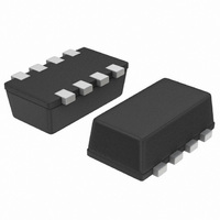
MOSFET PWR P-CH DUAL 8V CHIPFET
Manufacturer
ON Semiconductor
Datasheet
1.NTHD2102PT1G.pdf
(6 pages)
Specifications of NTHD2102PT1G
Fet Type
2 P-Channel (Dual)
Fet Feature
Logic Level Gate
Rds On (max) @ Id, Vgs
58 mOhm @ 3.4A, 4.5V
Drain To Source Voltage (vdss)
8V
Current - Continuous Drain (id) @ 25° C
3.4A
Vgs(th) (max) @ Id
1.5V @ 250µA
Gate Charge (qg) @ Vgs
16nC @ 2.5V
Input Capacitance (ciss) @ Vds
715pF @ 6.4V
Power - Max
1.1W
Mounting Type
Surface Mount
Package / Case
8-ChipFET™
Configuration
Dual Dual Drain
Transistor Polarity
P-Channel
Resistance Drain-source Rds (on)
0.058 Ohm @ 4.5 V
Forward Transconductance Gfs (max / Min)
8 S
Drain-source Breakdown Voltage
8 V
Gate-source Breakdown Voltage
+/- 8 V
Continuous Drain Current
3.4 A
Power Dissipation
1100 mW
Maximum Operating Temperature
+ 150 C
Mounting Style
SMD/SMT
Minimum Operating Temperature
- 55 C
Lead Free Status / RoHS Status
Lead free / RoHS Compliant
Other names
NTHD2102PT1GOS
NTHD2102PT1GOS
NTHD2102PT1GOSTR
NTHD2102PT1GOS
NTHD2102PT1GOSTR
Available stocks
Company
Part Number
Manufacturer
Quantity
Price
Company:

Part Number:
NTHD2102PT1G
Manufacturer:
ON
Quantity:
36 000
Part Number:
NTHD2102PT1G
Manufacturer:
ON/安森美
Quantity:
20 000


2. Pulse Test: Pulse Width = 250 ms, Duty Cycle = 2%.
3. Switching characteristics are independent of operating junction temperatures.
ELECTRICAL CHARACTERISTICS
OFF CHARACTERISTICS
ON CHARACTERISTICS (Note 2)
DYNAMIC CHARACTERISTICS
SWITCHING CHARACTERISTICS (Note 3
Drain−to−Source Breakdown Voltage (Note 2)
Gate−Body Leakage Current Zero
Zero Gate Voltage Drain Current
Gate Threshold Voltage
Static Drain−to−Source On−Resistance
Forward Transconductance
Diode Forward Voltage
Input Capacitance
Output Capacitance
Transfer Capacitance
Turn−On Delay Time
Rise Time
Turn−Off Delay Time
Fall Time
Gate Charge
Source−Drain Reverse Recovery Time
Temperature Coefficient (Positive)
Characteristic
(T
J
= 25°C unless otherwise noted)
Symbol
V
R
V
(Br)DSS
t
t
I
I
C
DS(on)
V
C
GS(th)
C
Q
g
d(on)
d(off)
Q
GSS
DSS
Q
t
FS
oss
t
t
SD
rss
http://onsemi.com
iss
rr
gs
gd
r
f
g
NTHD2102P
2
V
V
V
V
V
V
V
V
V
I
DS
GS
GS
GS
DS
I
DS
DS
F
GS
DS
S
= −0.9 A, di/dt = 100
= −1.1 A, V
= 0 V, V
= −4.5 V, I
= −2.5 V, I
= −1.8 V, I
= −5.0 V, I
Test Condition
= −6.4 V, V
= V
= −6.4 V, V
= 0 V, I
V
V
V
V
V
f = 1.0 MHz
R
I
I
DS
V
DD
GS
GS
DS
T
D
D
GS
G
J
GS
= −3.2 A
= −3.2 A
= 85°C
= −6.4 V
= 2.0 W
= −6.4 V
= −6.4 V
= −4.5 V
= −2.5 V
, I
= 0 V
D
GS
D
= −250 mA
= −250 mA
D
D
D
D
GS
= "8.0 V
GS
GS
= −3.4 A
= −2.7 A
= −1.0 A
= −3.4 A
= 0 V
= 0 V,
= 0 V
−0.45
−8.0
Min
−
−
−
−
−
−
−
−
−0.8
Typ
100
715
160
120
8.0
8.0
8.0
2.2
4.0
50
68
20
20
15
15
−
−
−
−
−
"100
Max
−1.0
−5.0
−1.5
−1.2
160
58
85
16
30
−
−
−
−
−
−
−
−
−
−
−
Unit
mW
nC
nA
mA
pF
nA
ns
V
V
S
V
Related parts for NTHD2102PT1G
Image
Part Number
Description
Manufacturer
Datasheet
Request
R

Part Number:
Description:
ON Semiconductor [VOLTAGE REGULATOR]
Manufacturer:
ON Semiconductor
Datasheet:
Part Number:
Description:
357-036-542-201 CARDEDGE 36POS DL .156 BLK LOPRO
Manufacturer:
ON Semiconductor
Datasheet:
Part Number:
Description:
357-036-542-201 CARDEDGE 36POS DL .156 BLK LOPRO
Manufacturer:
ON Semiconductor
Datasheet:
Part Number:
Description:
357-036-542-201 CARDEDGE 36POS DL .156 BLK LOPRO
Manufacturer:
ON Semiconductor
Datasheet:
Part Number:
Description:
357-036-542-201 CARDEDGE 36POS DL .156 BLK LOPRO
Manufacturer:
ON Semiconductor
Datasheet:
Part Number:
Description:
357-036-542-201 CARDEDGE 36POS DL .156 BLK LOPRO
Manufacturer:
ON Semiconductor
Datasheet:
Part Number:
Description:
357-036-542-201 CARDEDGE 36POS DL .156 BLK LOPRO
Manufacturer:
ON Semiconductor
Datasheet:
Part Number:
Description:
357-036-542-201 CARDEDGE 36POS DL .156 BLK LOPRO
Manufacturer:
ON Semiconductor
Datasheet:
Part Number:
Description:
357-036-542-201 CARDEDGE 36POS DL .156 BLK LOPRO
Manufacturer:
ON Semiconductor
Datasheet:
Part Number:
Description:
357-036-542-201 CARDEDGE 36POS DL .156 BLK LOPRO
Manufacturer:
ON Semiconductor
Datasheet:
Part Number:
Description:
357-036-542-201 CARDEDGE 36POS DL .156 BLK LOPRO
Manufacturer:
ON Semiconductor
Datasheet:
Part Number:
Description:
Manufacturer:
ON Semiconductor
Datasheet:
Part Number:
Description:
Manufacturer:
ON Semiconductor
Datasheet:
Part Number:
Description:
Manufacturer:
ON Semiconductor
Datasheet: