2N7002TA Diodes Zetex, 2N7002TA Datasheet - Page 2
2N7002TA
Manufacturer Part Number
2N7002TA
Description
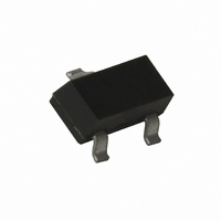
MOSFET N-CH 60V 115MA SOT23-3
Manufacturer
Diodes Zetex
Type
Small Signalr
Specifications of 2N7002TA
Fet Type
MOSFET N-Channel, Metal Oxide
Fet Feature
Standard
Rds On (max) @ Id, Vgs
7.5 Ohm @ 500mA, 10V
Drain To Source Voltage (vdss)
60V
Current - Continuous Drain (id) @ 25° C
115mA
Vgs(th) (max) @ Id
2.5V @ 250µA
Input Capacitance (ciss) @ Vds
50pF @ 25V
Power - Max
330mW
Mounting Type
Surface Mount
Package / Case
SOT-23-3, TO-236-3, Micro3™, SSD3, SST3
Number Of Elements
1
Polarity
N
Channel Mode
Enhancement
Drain-source On-res
7.5Ohm
Drain-source On-volt
60V
Gate-source Voltage (max)
±20V
Drain Current (max)
115mA
Output Power (max)
Not RequiredW
Frequency (max)
Not RequiredMHz
Noise Figure
Not RequireddB
Power Gain
Not RequireddB
Drain Efficiency
Not Required%
Operating Temp Range
-55C to 150C
Operating Temperature Classification
Military
Mounting
Surface Mount
Pin Count
3
Package Type
SOT-23
Power Dissipation
300mW
Continuous Drain Current
115mA
Lead Free Status / RoHS Status
Lead free / RoHS Compliant
Gate Charge (qg) @ Vgs
-
Lead Free Status / Rohs Status
Compliant
Other names
2N7002TR
Available stocks
Company
Part Number
Manufacturer
Quantity
Price
Company:

Part Number:
2N7002TA
Manufacturer:
ZTX
Quantity:
375 000
Company:
Part Number:
2N7002TA
Manufacturer:
ZETEX
Quantity:
586


Thermal Characteristics
Electrical Characteristics
Maximum Ratings
Drain-Source Voltage
Drain-Gate Voltage R
Gate-Source Voltage
Drain Current (Note 4)
Total Power Dissipation (Note 4)
Derating above T
Thermal Resistance, Junction to Ambient
Operating and Storage Temperature Range
OFF CHARACTERISTICS (Note 5)
Drain-Source Breakdown Voltage
Zero Gate Voltage Drain Current
Gate-Body Leakage
ON CHARACTERISTICS (Note 5)
Gate Threshold Voltage
Static Drain-Source On-Resistance
On-State Drain Current
Forward Transconductance
Diode Forward Voltage (Note 6)
Continuous Source Current (Note 6)
Pulse Source Current (Note 6)
DYNAMIC CHARACTERISTICS
Input Capacitance
Output Capacitance
Reverse Transfer Capacitance
SWITCHING CHARACTERISTICS
Turn-On Delay Time
Turn-Off Delay Time
Notes:
2N7002
Document number: DS11303 Rev. 24 - 2
4. Device mounted on FR-4 PCB 1.0 x 0.75 x 0.062 inch pad layout as shown on Diodes, Inc. suggested pad layout AP02001, which can be found on our
5. Short duration pulse test used to minimize self-heating effect.
6. V
website at http://www.diodes.com/datasheets/ap02001.pdf.
SD
measured in 250μs pulse, duty cycle = 2%; I
A
= 25°C
GS
≤ 1.0MΩ
Characteristic
Characteristic
Characteristic
@T
A
= 25°C unless otherwise specified
@T
@T
Continuous @ 100°C
A
A
= 25°C unless otherwise specified
= 25°C unless otherwise specified
@ T
@ T
@ T
@ T
Continuous
Continuous
SD
C
J
C
J
= 125°C
= 125°C
= 25°C
= 25°C
measure in 10ms Repetitive Pulse, duty cycle = 2% , Pd_Pulse is from Zth test data
Pulsed
Pulsed
www.diodes.com
Symbol
R
2 of 5
BV
V
t
I
t
D(OFF)
DS (ON)
I
I
D(ON)
C
D(ON)
V
C
C
GS(th)
g
DSS
GSS
I
I
SD
FS
SD
oss
DSS
S
iss
rss
Symbol
Symbol
T
V
J,
V
V
R
P
DSS
DGR
GSS
I
T
θ JA
D
D
STG
Min
1.0
0.5
60
80
⎯
⎯
⎯
⎯
⎯
⎯
⎯
⎯
⎯
⎯
⎯
0.78
Typ
3.2
4.4
1.0
2.0
7.0
70
22
11
11
⎯
⎯
⎯
⎯
⎯
⎯
-55 to +150
Max
13.5
500
±10
200
1.0
2.5
7.5
5.0
1.5
50
25
20
20
⎯
⎯
⎯
Value
Value
2
±20
±40
115
800
300
417
2.4
60
60
73
Unit
mS
mA
µA
nA
pF
pF
pF
ns
ns
Ω
V
V
A
V
A
V
V
V
V
V
V
V
V
V
V
f = 1.0MHz
V
R
R
GS
DS
GS
DS
GS
GS
GS
DS
GS
DS
DD
L
GEN
= 150Ω, V
Test Condition
= 60V, V
= V
=10V, I
= 30V, I
= 0V, I
= ±20V, V
= 5.0V, I
= 10V, I
= 10V, V
= 0V, I
= 25V, V
= 25Ω
GS
© Diodes Incorporated
mW/°C
November 2010
Units
Units
°C/W
mW
mA
, I
°C
2N7002
D
S
⎯
⎯
V
V
V
D
D
D
D
= 115mA
= 10μA
D
GS
DS
GS
GEN
= 0.2A
= 250μA
= 0.5A
= 0.2A,
DS
= 0.05A
= 0V
= 7.5V
= 0V
= 0V
= 10V,
Related parts for 2N7002TA
Image
Part Number
Description
Manufacturer
Datasheet
Request
R


Part Number:
Description:
DIODE ZENER 13V 500MW SOD-123
Manufacturer:
Diodes Zetex
Datasheet:

Part Number:
Description:
DIODE ZENER 13V 200MW SOD-323
Manufacturer:
Diodes Zetex
Datasheet:

Part Number:
Description:
DIODE ZENER 27V 500MW MINIMELF
Manufacturer:
Diodes Zetex
Datasheet:
Part Number:
Description:
DIODE ZENER 16V 200MW SOD-323
Manufacturer:
Diodes Zetex
Datasheet:
Part Number:
Description:
DIODE ZENER 28V 500MW SOD-123
Manufacturer:
Diodes Zetex
Datasheet:

Part Number:
Description:
DIODE ZENER 6.2V 200MW SC70-3
Manufacturer:
Diodes Zetex
Datasheet:

Part Number:
Description:
DIODE ZENER 3.6V 350MW SOT23-3
Manufacturer:
Diodes Zetex
Datasheet:

Part Number:
Description:
DIODE ZENER 4.3V 350MW SOT23-3
Manufacturer:
Diodes Zetex
Datasheet:
Part Number:
Description:
DIODE ZENER 13V 350MW SOT23-3
Manufacturer:
Diodes Zetex
Datasheet:
Part Number:
Description:
DIODE ZENER 16V 350MW SOT23-3
Manufacturer:
Diodes Zetex
Datasheet:

Part Number:
Description:
DIODE SW ARRAY 80V 200MW SOT363
Manufacturer:
Diodes Zetex
Datasheet:

Part Number:
Description:
DIODE SCHOTTKY 45V16A TO220-3
Manufacturer:
Diodes Zetex
Datasheet:
Part Number:
Description:
DIODE SCHOTTKY 45V 20A TO220-3
Manufacturer:
Diodes Zetex
Datasheet:
Part Number:
Description:
DIODE SW FAST DUAL CC SOT23-3
Manufacturer:
Diodes Zetex
Datasheet: