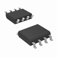
SI4431BDY-T1-E3 Vishay, SI4431BDY-T1-E3 Datasheet - Page 7

SI4431BDY-T1-E3
Manufacturer Part Number
SI4431BDY-T1-E3
Description
MOSFET P-CH 30V 5.7A 8-SOIC
Manufacturer
Vishay
Series
TrenchFET®r
Type
Power MOSFETr
Specifications of SI4431BDY-T1-E3
Transistor Polarity
P-Channel
Fet Type
MOSFET P-Channel, Metal Oxide
Fet Feature
Logic Level Gate
Rds On (max) @ Id, Vgs
30 mOhm @ 7.5A, 10V
Drain To Source Voltage (vdss)
30V
Current - Continuous Drain (id) @ 25° C
5.7A
Vgs(th) (max) @ Id
3V @ 250µA
Gate Charge (qg) @ Vgs
20nC @ 5V
Power - Max
1.5W
Mounting Type
Surface Mount
Package / Case
8-SOIC (3.9mm Width)
Minimum Operating Temperature
- 55 C
Configuration
Single Quad Drain Triple Source
Resistance Drain-source Rds (on)
0.03 Ohm @ 10 V
Drain-source Breakdown Voltage
30 V
Gate-source Breakdown Voltage
+/- 20 V
Continuous Drain Current
5.7 A
Power Dissipation
1500 mW
Maximum Operating Temperature
+ 150 C
Mounting Style
SMD/SMT
Continuous Drain Current Id
-7.5A
Drain Source Voltage Vds
-30V
On Resistance Rds(on)
50mohm
Rds(on) Test Voltage Vgs
-4.5V
Threshold Voltage Vgs Typ
-1V
Power Dissipation Pd
2.5W
Number Of Elements
1
Polarity
P
Channel Mode
Enhancement
Drain-source On-res
0.03Ohm
Drain-source On-volt
30V
Gate-source Voltage (max)
±20V
Operating Temp Range
-55C to 150C
Operating Temperature Classification
Military
Mounting
Surface Mount
Pin Count
8
Package Type
SOIC N
Lead Free Status / RoHS Status
Lead free / RoHS Compliant
Lead Free Status / RoHS Status
Lead free / RoHS Compliant, Lead free / RoHS Compliant
Other names
SI4431BDY-T1-E3TR
Available stocks
Company
Part Number
Manufacturer
Quantity
Price
Company:
Part Number:
SI4431BDY-T1-E3
Manufacturer:
VISHAY
Quantity:
2 500
Company:
Part Number:
SI4431BDY-T1-E3
Manufacturer:
VISHAY
Quantity:
37 500
Company:
Part Number:
SI4431BDY-T1-E3
Manufacturer:
VISHAY
Quantity:
20 000
Part Number:
SI4431BDY-T1-E3
Manufacturer:
VISHAY/威世
Quantity:
20 000
Wharton McDaniel
Surface-mounted LITTLE FOOT power MOSFETs use
integrated circuit and small-signal packages which have
been been modified to provide the heat transfer capabilities
required by power devices. Leadframe materials and
design, molding compounds, and die attach materials have
been changed, while the footprint of the packages remains
the same.
See Application Note 826, Recommended Minimum Pad
Patterns With Outline Drawing Access for Vishay Siliconix
MOSFETs, (http://www.vishay.com/ppg?72286), for the
basis of the pad design for a LITTLE FOOT SO-8 power
MOSFET. In converting this recommended minimum pad
to the pad set for a power MOSFET, designers must make
two connections: an electrical connection and a thermal
connection, to draw heat away from the package.
In the case of the SO-8 package, the thermal connections
are very simple. Pins 5, 6, 7, and 8 are the drain of the
MOSFET for a single MOSFET package and are connected
together. In a dual package, pins 5 and 6 are one drain, and
pins 7 and 8 are the other drain. For a small-signal device or
integrated circuit, typical connections would be made with
traces that are 0.020 inches wide. Since the drain pins serve
the additional function of providing the thermal connection
to the package, this level of connection is inadequate. The
total cross section of the copper may be adequate to carry
the current required for the application, but it presents a
large thermal impedance. Also, heat spreads in a circular
fashion from the heat source. In this case the drain pins are
the heat sources when looking at heat spread on the PC
board.
Document Number: 70740
Revision: 18-Jun-07
TrenchFET
Mounting LITTLE FOOT
0.050
0.027
1.27
0.69
Figure 1. Single MOSFET SO-8 Pad
Pattern With Copper Spreading
®
0.078
1.98
Power MOSFETs
V I S H A Y S I L I C O N I X
0.288
7.3
5.07
0.2
0.196
5.0
®
, SO-8 Power MOSFETs
The minimum recommended pad patterns for the
single-MOSFET SO-8 with copper spreading (Figure 1) and
dual-MOSFET SO-8 with copper spreading (Figure 2) show
the starting point for utilizing the board area available for the
heat-spreading copper. To create this pattern, a plane of
copper overlies the drain pins. The copper plane connects
the drain pins electrically, but more importantly provides
planar copper to draw heat from the drain leads and start the
process of spreading the heat so it can be dissipated into the
ambient air. These patterns use all the available area
underneath the body for this purpose.
Since surface-mounted packages are small, and reflow
soldering is the most common way in which these are
affixed to the PC board, “thermal” connections from the
planar copper to the pads have not been used. Even if
additional planar copper area is used, there should be no
problems in the soldering process. The actual solder
connections are defined by the solder mask openings. By
combining the basic footprint with the copper plane on the
drain pins, the solder mask generation occurs automatically.
A final item to keep in mind is the width of the power traces.
The absolute minimum power trace width must be
determined by the amount of current it has to carry. For
thermal reasons, this minimum width should be at least
0.020 inches. The use of wide traces connected to the drain
plane provides a low impedance path for heat to move away
from the device.
0.050
0.027
1.27
0.69
Figure 2. Dual MOSFET SO-8 Pad Pattern
0.078
1.98
With Copper Spreading
0.288
7.3
Application Note 808
5.07
0.2
www.vishay.com
0.088
0.088
2.25
2.25
1


