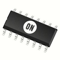
MC14536BDW ON Semiconductor, MC14536BDW Datasheet - Page 5

MC14536BDW
Manufacturer Part Number
MC14536BDW
Description
Timers & Support Products LOG CMOS OSILATR TIMER
Manufacturer
ON Semiconductor
Type
Programmabler
Datasheet
1.MC14536BCP.pdf
(14 pages)
Specifications of MC14536BDW
Number Of Internal Timers
1
Supply Voltage (max)
18 V
Supply Voltage (min)
3 V
Maximum Power Dissipation
500 mW
Maximum Operating Temperature
+ 125 C
Minimum Operating Temperature
- 55 C
Mounting Style
SMD/SMT
Propagation Delay (max)
3600 ns, 1300 ns, 1000 ns
Package / Case
SOIC-16 Wide
Lead Free Status / RoHS Status
Lead free / RoHS Compliant
Available stocks
Company
Part Number
Manufacturer
Quantity
Price
Company:
Part Number:
MC14536BDWG
Manufacturer:
ON
Quantity:
2 416
Part Number:
MC14536BDWR2
Manufacturer:
MOTOROLA/摩托罗拉
Quantity:
20 000
Company:
Part Number:
MC14536BDWR2G
Manufacturer:
Exar
Quantity:
714
Part Number:
MC14536BDWR2G
Manufacturer:
ON/安森美
Quantity:
20 000
INPUTS
Out to a high level. This is accomplished by setting an output
conditioning latch to a high level while at the same time
resetting the 24 flip−flop stages. After Set goes low (inactive),
the occurrence of the first negative clock transition on IN
causes Decode Out to go low. The counter’s flip−flop stages
begin counting on the second negative clock transition of IN
When Set is high, the on−chip RC oscillator is disabled. This
allows for very low−power standby operation.
Decode Out to a low level; all 24 flip−flop stages are also reset
to a low level. Like the Set input, Reset disables the on−chip
RC oscillator for standby operation.
negative−going edge of this input. IN
external clock input or used in conjunction with OUT
OUT
used, both OUT
to drive 1 LSTTL or several CMOS loads.
flip−flop stages to be bypassed. This device essentially
becomes a 16−stage counter with all 16 stages selectable.
Selection is accomplished by the A, B, C, and D inputs. (See
the truth tables.)
disconnects the first counter stage from the clocking source.
This holds the present count and inhibits further counting.
However, the clocking source may continue to run.
Therefore, when Clock Inhibit is brought low, no oscillator
startup time is required. When Clock Inhibit is low, the
counter will start counting on the occurrence of the first
negative edge of the clocking source at IN
8−Bypass
SET (Pin 1) − A high on Set asynchronously forces Decode
RESET (Pin 2) − A high on Reset asynchronously forces
IN
8−BYPASS (Pin 6) − A high on this input causes the first 8
CLOCK INHIBIT (Pin 7) − A high on this input
1
2
0
0
0
0
0
0
0
0
0
0
0
0
0
0
0
0
(Pin 3) − The device’s internal counters advance on the
to form an RC oscillator. When an external clock is
D
0
0
0
0
0
0
0
0
1
1
1
1
1
1
1
1
1
and OUT
Input
C
0
0
0
0
1
1
1
1
0
0
0
0
1
1
1
1
2
may be left unconnected or used
B
0
0
1
1
0
0
1
1
0
0
1
1
0
0
1
1
A
0
1
0
1
0
1
0
1
0
1
0
1
0
1
0
1
1
may be used as an
for Decode Out
1
Stage Selected
.
10
11
12
13
14
15
16
17
18
19
20
21
22
23
24
9
PIN DESCRIPTIONS
http://onsemi.com
TRUTH TABLES
1
and
MC14536B
1
1
.
5
RC oscillator which allows for very low−power standby
operation. May also be used, in conjunction with an external
clock, with essentially the same results as the Clock Inhibit
input.
on−chip monostable multivibrator. If the Mono−In input is
connected to V
Decode Out is directly connected to the selected Q output.
The monostable circuit is enabled if a resistor is connected
between Mono−In and V
internal capacitance will determine the minimum output
pulse widths. With the addition of an external capacitor to
V
operation the resistor value should be limited to the range of
5 kW to 100 kW and the capacitor value should be limited to
a maximum of 1000 pf. (See figures 5, 6, 7, and 12).
flip−flop stage to be connected to Decode Out. (See the truth
tables.)
OUTPUTS
IN
may be used for 2
configuration. When the monostable circuit is disabled, this
output is a 50% duty cycle square wave during free run.
TEST MODE
stages into three 8−stage sections to facilitate a fast test
sequence. The test mode is enabled when 8−Bypass, Set and
Reset are at a high level. (See Figure 10.)
8−Bypass
SS
OSC INHIBIT (Pin 14) − A high level on this pin stops the
MONO−IN (Pin 15) − Used as the timing pin for the
A, B, C, D (Pins 9, 10, 11, 12) − These inputs select the
OUT
DECODE OUT (Pin 13) − Output function depends on
The test mode configuration divides the 24 flip−flop
1
, the pulse width range may be extended. For reliable
to form an RC oscillator. These outputs are buffered and
1
1
1
1
1
1
1
1
1
1
1
1
1
1
1
1
1
, OUT
D
2
0
0
0
0
0
0
0
0
1
1
1
1
1
1
1
1
SS
(Pin 4, 5) − Outputs used in conjunction with
Input
, the monostable circuit is disabled, and
0
frequency division of an external clock.
C
0
0
0
0
1
1
1
1
0
0
0
0
1
1
1
1
DD
. This resistor and the device’s
B
0
0
1
1
0
0
1
1
0
0
1
1
0
0
1
1
A
0
1
0
1
0
1
0
1
0
1
0
1
0
1
0
1
Stage Selected
for Decode Out
10
12
13
14
15
16
11
1
2
3
4
5
6
7
8
9


