IRF820ASPBF Vishay, IRF820ASPBF Datasheet - Page 6
IRF820ASPBF
Manufacturer Part Number
IRF820ASPBF
Description
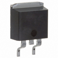
MOSFET N-CH 500V 2.5A D2PAK
Manufacturer
Vishay
Datasheet
1.IRF820ASPBF.pdf
(11 pages)
Specifications of IRF820ASPBF
Transistor Polarity
N-Channel
Fet Type
MOSFET N-Channel, Metal Oxide
Fet Feature
Standard
Rds On (max) @ Id, Vgs
3 Ohm @ 1.5A, 10V
Drain To Source Voltage (vdss)
500V
Current - Continuous Drain (id) @ 25° C
2.5A
Vgs(th) (max) @ Id
4.5V @ 250µA
Gate Charge (qg) @ Vgs
17nC @ 10V
Input Capacitance (ciss) @ Vds
340pF @ 25V
Power - Max
50W
Mounting Type
Surface Mount
Package / Case
D²Pak, TO-263 (2 leads + tab)
Minimum Operating Temperature
- 55 C
Configuration
Single
Resistance Drain-source Rds (on)
3 Ohm @ 10 V
Drain-source Breakdown Voltage
500 V
Gate-source Breakdown Voltage
+/- 30 V
Continuous Drain Current
2.5 A
Power Dissipation
50000 mW
Maximum Operating Temperature
+ 150 C
Mounting Style
SMD/SMT
Continuous Drain Current Id
2.5A
Drain Source Voltage Vds
500V
On Resistance Rds(on)
3ohm
Rds(on) Test Voltage Vgs
10V
Leaded Process Compatible
Yes
Lead Free Status / RoHS Status
Lead free / RoHS Compliant
Lead Free Status / RoHS Status
Lead free / RoHS Compliant, Lead free / RoHS Compliant
Other names
*IRF820ASPBF


Document Number: 91058
Fig 12a. Unclamped Inductive Test Circuit
Fig 12b. Unclamped Inductive Waveforms
Fig 13b. Gate Charge Test Circuit
Fig 13a. Basic Gate Charge Waveform
I
AS
12V
V
V
G
GS
R G
20V
Same Type as D.U.T.
V DS
Current Regulator
Q
.2µF
GS
t p
t p
50KΩ
3mA
Current Sampling Resistors
I AS
.3µF
D.U.T
0.01 Ω
L
I
G
Q
Charge
Q
V
GD
G
(BR)DSS
D.U.T.
I
D
15V
+
-
V
DS
DRIVER
+
-
V DD
A
300
250
200
150
100
700
650
600
550
50
Fig 12d. Typical Drain-to-Source Voltage
0
25
Fig 12c. Maximum Avalanche Energy
0.0
Starting T , Junction Temperature ( C)
0.5
50
Vs. Avalanche Current
I AV , Avalanche Current ( A)
Vs. Drain Current
J
1.0
75
1.5
100
TOP
BOTTOM
www.vishay.com
2.0
125
°
1.1A
1.6A
2.5A
I D
2.5
150
6
Related parts for IRF820ASPBF
Image
Part Number
Description
Manufacturer
Datasheet
Request
R

Part Number:
Description:
N CHANNEL MOSFET, 500V, 2.5A TO-220
Manufacturer:
Vishay
Datasheet:
Part Number:
Description:
MOSFET N-CH 500V 2.5A TO-220AB
Manufacturer:
Vishay
Datasheet:

Part Number:
Description:
357-036-542-201 CARDEDGE 36POS DL .156 BLK LOPRO
Manufacturer:
Vishay
Datasheet:
Part Number:
Description:
357-036-542-201 CARDEDGE 36POS DL .156 BLK LOPRO
Manufacturer:
Vishay
Datasheet:
Part Number:
Description:
357-036-542-201 CARDEDGE 36POS DL .156 BLK LOPRO
Manufacturer:
Vishay
Datasheet:
Part Number:
Description:
357-036-542-201 CARDEDGE 36POS DL .156 BLK LOPRO
Manufacturer:
Vishay
Datasheet:
Part Number:
Description:
357-036-542-201 CARDEDGE 36POS DL .156 BLK LOPRO
Manufacturer:
Vishay
Datasheet:
Part Number:
Description:
357-036-542-201 CARDEDGE 36POS DL .156 BLK LOPRO
Manufacturer:
Vishay
Datasheet:
Part Number:
Description:
357-036-542-201 CARDEDGE 36POS DL .156 BLK LOPRO
Manufacturer:
Vishay
Datasheet:
Part Number:
Description:
357-036-542-201 CARDEDGE 36POS DL .156 BLK LOPRO
Manufacturer:
Vishay
Datasheet:
Part Number:
Description:
357-036-542-201 CARDEDGE 36POS DL .156 BLK LOPRO
Manufacturer:
Vishay
Datasheet:
Part Number:
Description:
357-036-542-201 CARDEDGE 36POS DL .156 BLK LOPRO
Manufacturer:
Vishay
Datasheet:
Part Number:
Description:
357-036-542-201 CARDEDGE 36POS DL .156 BLK LOPRO
Manufacturer:
Vishay
Datasheet:
Part Number:
Description:
357-036-542-201 CARDEDGE 36POS DL .156 BLK LOPRO
Manufacturer:
Vishay
Datasheet:
Part Number:
Description:
357-036-542-201 CARDEDGE 36POS DL .156 BLK LOPRO
Manufacturer:
Vishay
Datasheet: