IRFU4615PBF International Rectifier, IRFU4615PBF Datasheet - Page 2
IRFU4615PBF
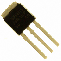
Manufacturer Part Number
IRFU4615PBF
Description
MOSFET N-CH 150V 33A IPAK
Manufacturer
International Rectifier
Series
HEXFET®r
Datasheet
1.IRFU4615PBF.pdf
(11 pages)
Specifications of IRFU4615PBF
Fet Type
MOSFET N-Channel, Metal Oxide
Fet Feature
Standard
Rds On (max) @ Id, Vgs
42 mOhm @ 21A, 10V
Drain To Source Voltage (vdss)
150V
Current - Continuous Drain (id) @ 25° C
33A
Vgs(th) (max) @ Id
5V @ 100µA
Gate Charge (qg) @ Vgs
26nC @ 10V
Input Capacitance (ciss) @ Vds
1750pF @ 50V
Power - Max
144W
Mounting Type
Through Hole
Package / Case
IPak, TO-251, DPak, VPak (3 straight leads + tab)
Transistor Polarity
N-Channel
Drain-source Breakdown Voltage
150 V
Gate-source Breakdown Voltage
20 V
Continuous Drain Current
33 A
Power Dissipation
144 W
Mounting Style
SMD/SMT
Gate Charge Qg
26 nC
Lead Free Status / RoHS Status
Lead free / RoHS Compliant


V
∆V
R
V
I
I
R
gfs
Q
Q
Q
Q
t
t
t
t
C
C
C
C
C
I
I
V
t
Q
I
t
Static @ T
Dynamic @ T
Diode Characteristics
DSS
GSS
d(on)
r
d(off)
f
S
SM
rr
RRM
on
(BR)DSS
DS(on)
GS(th)
G(int)
iss
oss
rss
oss
oss
SD
g
gs
gd
sync
rr
Symbol
Symbol
Symbol
2
(BR)DSS
eff. (ER) Effective Output Capacitance (Energy Related)
eff. (TR) Effective Output Capacitance (Time Related)
/∆T
J
J
Drain-to-Source Breakdown Voltage
Breakdown Voltage Temp. Coefficient
Static Drain-to-Source On-Resistance
Gate Threshold Voltage
Drain-to-Source Leakage Current
Gate-to-Source Forward Leakage
Gate-to-Source Reverse Leakage
Internal Gate Resistance
Forward Transconductance
Total Gate Charge
Gate-to-Source Charge
Gate-to-Drain ("Miller") Charge
Total Gate Charge Sync. (Q
Turn-On Delay Time
Rise Time
Turn-Off Delay Time
Fall Time
Input Capacitance
Output Capacitance
Reverse Transfer Capacitance
Continuous Source Current
(Body Diode)
Pulsed Source Current
(Body Diode)
Diode Forward Voltage
Reverse Recovery Time
Reverse Recovery Charge
Reverse Recovery Current
Forward Turn-On Time
= 25°C (unless otherwise specified)
J
= 25°C (unless otherwise specified)
Parameter
Ù
Parameter
Parameter
g
- Q
gd
)
g
Ã
Intrinsic turn-on time is negligible (turn-on is dominated by LS+LD)
Min. Typ. Max. Units
Min. Typ. Max. Units
Min. Typ. Max. Units
150
–––
–––
–––
–––
–––
–––
–––
–––
–––
–––
–––
–––
–––
–––
–––
–––
–––
–––
–––
–––
–––
–––
–––
–––
–––
–––
–––
3.0
–––
35
1750
0.19
–––
155
–––
–––
–––
–––
–––
–––
179
382
–––
–––
–––
177
247
2.7
8.6
9.0
4.9
34
26
17
15
35
25
20
40
70
83
-100
–––
–––
250
100
–––
–––
–––
–––
–––
–––
–––
–––
–––
–––
–––
–––
–––
–––
140
–––
–––
–––
–––
–––
5.0
1.3
42
20
33
V/°C
mΩ
µA
nA
nC
pF
nC
ns
ns
Ω
A
V
V
S
V
A
V
Reference to 25°C, I
V
V
V
V
V
V
V
I
V
V
I
V
I
R
V
V
V
ƒ = 1.0MHz
V
V
MOSFET symbol
showing the
integral reverse
p-n junction diode.
T
T
T
T
T
T
D
D
D
J
J
J
J
J
J
GS
GS
DS
DS
DS
GS
GS
DS
DS
GS
DD
GS
GS
DS
GS
GS
G
= 21A
= 21A, V
= 21A
= 25°C, I
= 25°C
= 125°C
= 25°C
= 125°C
= 25°C
= 7.3Ω
= V
= 150V, V
= 150V, V
= 50V, I
= 75V
= 50V
= 0V, I
= 10V, I
= 20V
= -20V
= 10V
= 98V
= 10V
= 0V
= 0V, V
= 0V, V
GS
, I
D
f
f
DS
D
S
DS
DS
D
D
= 250µA
= 21A, V
= 100µA
= 21A
=0V, V
= 21A
GS
GS
= 0V to 120V
= 0V to 120V
Conditions
Conditions
Conditions
(See Fig.5)
= 0V
= 0V, T
V
I
di/dt = 100A/µs
F
R
= 21A
D
f
GS
= 100V,
GS
= 5mA
= 10V
J
= 0V
= 125°C
www.irf.com
g
™
G
f
(See Fig.11)
f
S
D
Related parts for IRFU4615PBF
Image
Part Number
Description
Manufacturer
Datasheet
Request
R

Part Number:
Description:
SCHOTTKY RECTIFIER
Manufacturer:
International Rectifier Corp.
Datasheet:
Part Number:
Description:
SCHOTTKY RECTIFIER
Manufacturer:
International Rectifier Corp.
Datasheet:
Part Number:
Description:
SCHOTTKY RECTIFIER
Manufacturer:
International Rectifier Corp.
Datasheet:
Part Number:
Description:
SCHOTTKY RECTIFIER
Manufacturer:
International Rectifier Corp.
Datasheet:
Part Number:
Description:
SCHOTTKY RECTIFIER
Manufacturer:
International Rectifier Corp.
Datasheet:
Part Number:
Description:
SCHOTTKY RECTIFIER
Manufacturer:
International Rectifier Corp.
Datasheet:
Part Number:
Description:
SCHOTTKY RECTIFIER
Manufacturer:
International Rectifier Corp.
Datasheet:
Part Number:
Description:
SCHOTTKY RECTIFIER
Manufacturer:
International Rectifier Corp.
Datasheet:
Part Number:
Description:
SCHOTTKY RECTIFIER
Manufacturer:
International Rectifier Corp.
Datasheet:
Part Number:
Description:
SCHOTTKY RECTIFIER
Manufacturer:
International Rectifier Corp.
Datasheet:
Part Number:
Description:
SCHOTTKY RECTIFIER
Manufacturer:
International Rectifier Corp.
Datasheet:
Part Number:
Description:
SCHOTTKY RECTIFIER
Manufacturer:
International Rectifier Corp.
Datasheet:
Part Number:
Description:
SCHOTTKY RECTIFIER
Manufacturer:
International Rectifier Corp.
Datasheet:
Part Number:
Description:
SCHOTTKY RECTIFIER
Manufacturer:
International Rectifier Corp.
Datasheet:
Part Number:
Description:
SCHOTTKY RECTIFIER
Manufacturer:
International Rectifier Corp.
Datasheet: