RJK03B9DPA-00#J53 Renesas Electronics America, RJK03B9DPA-00#J53 Datasheet - Page 4
RJK03B9DPA-00#J53
Manufacturer Part Number
RJK03B9DPA-00#J53
Description
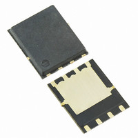
MOSFET N-CH 30V 30A W-PAK
Manufacturer
Renesas Electronics America
Datasheet
1.RJK03B9DPA-00J53.pdf
(7 pages)
Specifications of RJK03B9DPA-00#J53
Fet Type
MOSFET N-Channel, Metal Oxide
Fet Feature
Logic Level Gate
Rds On (max) @ Id, Vgs
10.6 mOhm @ 15A, 10V
Drain To Source Voltage (vdss)
30V
Current - Continuous Drain (id) @ 25° C
30A
Gate Charge (qg) @ Vgs
7.4nC @ 4.5V
Input Capacitance (ciss) @ Vds
1110pF @ 10V
Power - Max
25W
Mounting Type
Surface Mount
Package / Case
WPAK
Lead Free Status / RoHS Status
Lead free / RoHS Compliant
Vgs(th) (max) @ Id
-
Other names
RJK03B9DPA-00#J53TR
Available stocks
Company
Part Number
Manufacturer
Quantity
Price


RJK03B9DPA
REJ03G1791-0320 Rev.3.20
May 12, 2010
Static Drain to Source On State Resistance
10
50
40
30
20
10
20
16
12
8
6
4
2
0
0
8
4
0
–25
25
0
Pulse Test
V
Channel Temperature Tch (°C)
Maximum Avalanche Energy vs.
GS
Channel Temperature Derating
I
Dynamic Input Characteristics
D
Case Temperature Tc (°C)
V
0
= 30 A
DS
= 4.5 V
V
50
Gate Charge Qg (nc)
10 V
DD
8
25
= 25 V
vs. Temperature
I
10 V
D
16
75
= 5 A, 10 A, 20 A
50
V
DD
75
100
5 A, 10 A, 20 A
24
= 25 V
10 V
I
V
duty < 0.1%
Rg ≥ 50 Ω
AP
100 125 150
DD
= 8 A
= 15 V
125
32
V
GS
150
40
20
16
12
8
4
0
10000
3000
1000
300
100
30
10
50
40
30
20
10
0
0
Drain to Source Voltage V
Source to Drain Voltage V
V
f = 1 MHz
GS
Reverse Drain Current vs.
Drain to Source Voltage
= 0
Typical Capacitance vs.
0.4
Source to Drain Voltage
10 V
5 V
10
0.8
V
GS
1.2
= 0, –5 V
20
Pulse Test
1.6
Coss
Ciss
DS
Crss
SD
Preliminary
Page 4 of 6
(V)
(V)
30
2.0
Related parts for RJK03B9DPA-00#J53
Image
Part Number
Description
Manufacturer
Datasheet
Request
R

Part Number:
Description:
KIT STARTER FOR M16C/29
Manufacturer:
Renesas Electronics America
Datasheet:

Part Number:
Description:
KIT STARTER FOR R8C/2D
Manufacturer:
Renesas Electronics America
Datasheet:

Part Number:
Description:
R0K33062P STARTER KIT
Manufacturer:
Renesas Electronics America
Datasheet:

Part Number:
Description:
KIT STARTER FOR R8C/23 E8A
Manufacturer:
Renesas Electronics America
Datasheet:

Part Number:
Description:
KIT STARTER FOR R8C/25
Manufacturer:
Renesas Electronics America
Datasheet:

Part Number:
Description:
KIT STARTER H8S2456 SHARPE DSPLY
Manufacturer:
Renesas Electronics America
Datasheet:

Part Number:
Description:
KIT STARTER FOR R8C38C
Manufacturer:
Renesas Electronics America
Datasheet:

Part Number:
Description:
KIT STARTER FOR R8C35C
Manufacturer:
Renesas Electronics America
Datasheet:

Part Number:
Description:
KIT STARTER FOR R8CL3AC+LCD APPS
Manufacturer:
Renesas Electronics America
Datasheet:
Part Number:
Description:
KIT STARTER FOR RX610
Manufacturer:
Renesas Electronics America
Datasheet:

Part Number:
Description:
KIT STARTER FOR R32C/118
Manufacturer:
Renesas Electronics America
Datasheet:

Part Number:
Description:
KIT DEV RSK-R8C/26-29
Manufacturer:
Renesas Electronics America
Datasheet:

Part Number:
Description:
KIT STARTER FOR SH7124
Manufacturer:
Renesas Electronics America
Datasheet:

Part Number:
Description:
KIT STARTER FOR H8SX/1622
Manufacturer:
Renesas Electronics America
Datasheet:

Part Number:
Description:
KIT DEV FOR SH7203
Manufacturer:
Renesas Electronics America
Datasheet: