NTE4151PT1G ON Semiconductor, NTE4151PT1G Datasheet
NTE4151PT1G
Specifications of NTE4151PT1G
Available stocks


Related parts for NTE4151PT1G


NTE4151PT1G Summary of contents
Page 1
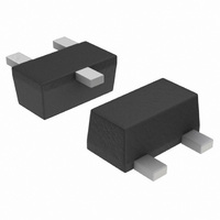
NTA4151P, NTE4151P Small Signal MOSFET −20 V, −760 mA, Single P−Channel, Gate Zener, SC−75, SC−89 Features • Low R for Higher Efficiency and Longer Battery Life DS(on) • Small Outline Package (1.6 x 1.6 mm) • SC−75 Standard Gullwing Package ...
Page 2
... Switching characteristics are independent of operating junction temperatures. ORDERING INFORMATION Device NTA4151PT1 NTA4151PT1G NTE4151PT1G †For information on tape and reel specifications, including part orientation and tape sizes, please refer to our Tape and Reel Packaging Specifications Brochure, BRD8011/D. NTA4151P, NTE4151P (T = 25°C unless otherwise stated) ...
Page 3
TYPICAL ELECTRICAL CHARACTERISTICS 0.7 0.6 −1 −1. −4 0.4 0.3 0.2 0 0.5 1.0 1.5 2.0 −V , DRAIN−TO−SOURCE VOLTAGE (VOLTS) DS Figure 1. On−Region Characteristics 0 −4.5 ...
Page 4
TYPICAL ELECTRICAL CHARACTERISTICS 0.4 0.8 1.2 1 TOTAL GATE CHARGE (nC) G Figure 7. Gate−to−Source Voltage vs. Total Gate Charge 1 0.5 0.2 ...
Page 5
... L A1 SOLDERING FOOTPRINT* 1.803 0.071 0.508 0.020 *For additional information on our Pb−Free strategy and soldering details, please download the ON Semiconductor Soldering and Mounting Techniques Reference Manual, SOLDERRM/D. SC−75/SOT−416 CASE 463−01 ISSUE F NOTES: 1. DIMENSIONING AND TOLERANCING PER ANSI Y14.5M, 1982. ...
Page 6
... *For additional information on our Pb−Free strategy and soldering details, please download the ON Semiconductor Soldering and Mounting Techniques Reference Manual, SOLDERRM/D. ON Semiconductor and are registered trademarks of Semiconductor Components Industries, LLC (SCILLC). SCILLC reserves the right to make changes without further notice to any products herein. SCILLC makes no warranty, representation or guarantee regarding the suitability of its products for any particular purpose, nor does SCILLC assume any liability arising out of the application or use of any product or circuit, and specifically disclaims any and all liability, including without limitation special, consequential or incidental damages. “ ...