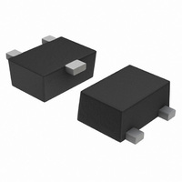
NTK3139PT1G ON Semiconductor, NTK3139PT1G Datasheet - Page 2

NTK3139PT1G
Manufacturer Part Number
NTK3139PT1G
Description
MOSFET P-CH 20V 660MA SOT-723
Manufacturer
ON Semiconductor
Datasheet
1.NTK3139PT1G.pdf
(5 pages)
Specifications of NTK3139PT1G
Fet Type
MOSFET P-Channel, Metal Oxide
Fet Feature
Logic Level Gate
Rds On (max) @ Id, Vgs
480 mOhm @ 780mA, 4.5V
Drain To Source Voltage (vdss)
20V
Current - Continuous Drain (id) @ 25° C
660mA
Vgs(th) (max) @ Id
1.2V @ 250µA
Input Capacitance (ciss) @ Vds
170pF @ 16V
Power - Max
310mW
Mounting Type
Surface Mount
Package / Case
SOT-723
Configuration
Single
Transistor Polarity
P-Channel
Resistance Drain-source Rds (on)
0.48 Ohm @ 4.5 V
Forward Transconductance Gfs (max / Min)
1.2 S
Drain-source Breakdown Voltage
20 V
Gate-source Breakdown Voltage
+/- 6 V
Continuous Drain Current
0.78 A
Power Dissipation
450 mW
Maximum Operating Temperature
+ 150 C
Mounting Style
SMD/SMT
Minimum Operating Temperature
- 55 C
Lead Free Status / RoHS Status
Lead free / RoHS Compliant
Gate Charge (qg) @ Vgs
-
Lead Free Status / Rohs Status
Lead free / RoHS Compliant
Other names
NTK3139PT1G
NTK3139PT1GOSTR
NTK3139PT1GOSTR
Available stocks
Company
Part Number
Manufacturer
Quantity
Price
Company:
Part Number:
NTK3139PT1G
Manufacturer:
ON
Quantity:
52 000
Company:
Part Number:
NTK3139PT1G
Manufacturer:
ON
Quantity:
30 000
Part Number:
NTK3139PT1G
Manufacturer:
ON/安森美
Quantity:
20 000
3. Surface mounted on FR4 board using 1 in sq pad size (Cu area = 1.127 in sq [1 oz] including traces)
4. Surface mounted on FR4 board using the minimum recommended pad size
5. Pulse Test: pulse width = 300 ms, duty cycle = 2%
6. Switching characteristics are independent of operating junction temperatures
MOSFET ELECTRICAL CHARACTERISTICS
OFF CHARACTERISTICS
ON CHARACTERISTICS (Note 5)
CHARGES, CAPACITANCES AND GATE RESISTANCE
SWITCHING CHARACTERISTICS, V
DRAIN SOURCE DIODE CHARACTERISTICS
THERMAL RESISTANCE RATINGS
Junction−to−Ambient – Steady State (Note 3)
Junction−to−Ambient – t = 5 s (Note 3)
Junction−to−Ambient – Steady State Minimum Pad (Note 4)
Drain−to−Source Breakdown
Voltage
Drain−to−Source Breakdown
Voltage Temperature Coefficient
Zero Gate Voltage Drain Current
Gate−to−Source Leakage Current
Gate Threshold Voltage
Negative Threshold Temperature
Coefficient
Drain−to−Source On Resistance
Forward Transconductance
Input Capacitance
Output Capacitance
Reverse Transfer Capacitance
Turn On Delay Time
Rise Time
TurnOff Delay Time
Fall Time
Forward Diode Voltage
Reverse Recovery Time
Charge Time
Discharge Time
Reverse Recovery Charge
Parameter
Parameter
GS
V
V
V
(BR)DSS
Symbol
= 4.5 V (Note 6)
V
GS(TH)
R
t
(BR)DSS
t
d(OFF)
C
C
I
I
d(ON)
Q
GS(TH)
C
V
GSS
DS(on)
t
DSS
g
RR
OSS
t
t
RSS
t
t
SD
RR
ISS
FS
a
b
r
f
/T
/T
J
J
(T
J
V
= 25°C unless otherwise specified)
http://onsemi.com
GS
V
I
D
GS
V
= 0 V, I
NTK3139P
V
= −250 mA, Reference to 25°C
V
V
V
V
GS
V
V
V
I
GS
I
V
V
= 0 V, f = 1 MHz, V
V
GS
GS
GS
GS
D
DS
DS
S
GS
DS
GS
GS
= 0 V, d
= −200 mA, R
= −1.0 A, V
= −4.5 V, V
= −4.5 V, I
= −2.5 V, I
= −1.8 V, I
= −1.5 V, I
= −16V
= −10 V, I
2
= 0 V,
Test Condition
S
= 0 V, V
= V
= 0 V, I
= −350 mA
DS
ISD
Symbol
, I
D
R
R
R
GS
/d
D
D
DD
D
D
D
D
= −250 mA
qJA
qJA
qJA
DS
= −250 mA
t
= −540 mA
= −780 mA
= −660 mA
= −100 mA
= −100 mA
= 100 A/ms,
= ±4.5 V
G
= −20 V
= −10 V,
= 10 W
DS
T
= −16 V
T
T
J
J
J
= 125°C
= 25°C
= 25°C
Max
280
228
400
−0.45
Min
−20
−16.5
32.7
20.3
−0.8
13.2
11.8
Typ
0.38
0.52
0.70
0.95
113
9.0
5.8
1.4
5.0
2.4
1.2
9.0
15
Max
−1.0
−2.0
±2.0
−1.2
−1.2
0.48
0.67
0.95
2.20
170
25
15
°C/W
Unit
mV/°C
mV/°C
Unit
mA
mA
nC
ns
ns
pF
V
V
W
V
S


