IRF840ASPBF Vishay, IRF840ASPBF Datasheet - Page 7
IRF840ASPBF
Manufacturer Part Number
IRF840ASPBF
Description
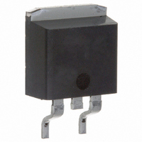
MOSFET N-CH 500V 8A D2PAK
Manufacturer
Vishay
Type
Power MOSFETr
Specifications of IRF840ASPBF
Transistor Polarity
N-Channel
Fet Type
MOSFET N-Channel, Metal Oxide
Fet Feature
Standard
Rds On (max) @ Id, Vgs
850 mOhm @ 4.8A, 10V
Drain To Source Voltage (vdss)
500V
Current - Continuous Drain (id) @ 25° C
8A
Vgs(th) (max) @ Id
4V @ 250µA
Gate Charge (qg) @ Vgs
38nC @ 10V
Input Capacitance (ciss) @ Vds
1018pF @ 25V
Power - Max
3.1W
Mounting Type
Surface Mount
Package / Case
D²Pak, TO-263 (2 leads + tab)
Minimum Operating Temperature
- 55 C
Configuration
Single
Resistance Drain-source Rds (on)
0.85 Ohm @ 10 V
Drain-source Breakdown Voltage
500 V
Gate-source Breakdown Voltage
+/- 30 V
Continuous Drain Current
8 A
Power Dissipation
3100 mW
Maximum Operating Temperature
+ 150 C
Mounting Style
SMD/SMT
Continuous Drain Current Id
8A
Drain Source Voltage Vds
500V
On Resistance Rds(on)
850mohm
Rds(on) Test Voltage Vgs
10V
Threshold Voltage Vgs Typ
4V
Number Of Elements
1
Polarity
N
Channel Mode
Enhancement
Drain-source On-res
0.85Ohm
Drain-source On-volt
500V
Gate-source Voltage (max)
±30V
Output Power (max)
Not RequiredW
Frequency (max)
Not RequiredMHz
Noise Figure
Not RequireddB
Power Gain
Not RequireddB
Drain Efficiency
Not Required%
Operating Temp Range
-55C to 150C
Operating Temperature Classification
Military
Mounting
Surface Mount
Pin Count
2 +Tab
Package Type
D2PAK
Lead Free Status / RoHS Status
Lead free / RoHS Compliant
Lead Free Status / RoHS Status
Lead free / RoHS Compliant, Lead free / RoHS Compliant
Other names
*IRF840ASPBF
Available stocks
Company
Part Number
Manufacturer
Quantity
Price


Document Number: 91066
Re-Applied
Voltage
Reverse
Recovery
Current
‚
+
-
R
D.U.T
G
*
Fig 14. For N-Channel HEXFET
Driver Gate Drive
D.U.T. I
D.U.T. V
Inductor Curent
V
GS
= 5V for Logic Level Devices
P.W.
SD
DS
Waveform
Waveform
Peak Diode Recovery dv/dt Test Circuit
Ripple ≤ 5%
Body Diode
Period
Body Diode Forward
+
-
ƒ
• dv/dt controlled by R
• Driver same type as D.U.T.
• I
• D.U.T. - Device Under Test
SD
Diode Recovery
Current
controlled by Duty Factor "D"
Circuit Layout Considerations
dv/dt
Forward Drop
• Low Stray Inductance
• Ground Plane
• Low Leakage Inductance
di/dt
Current Transformer
®
D =
-
Power MOSFETs
G
Period
„
P.W.
+
IRF840AS/LPbF
V
V
I
SD
GS
DD
=10V
+
-
V
DD
*
www.vishay.com
7
Related parts for IRF840ASPBF
Image
Part Number
Description
Manufacturer
Datasheet
Request
R

Part Number:
Description:
MOSFET N-CH 500V 8A TO-220AB
Manufacturer:
Vishay
Datasheet:
Part Number:
Description:
MOSFET N-CH 500V 8A TO-220AB
Manufacturer:
Vishay
Datasheet:

Part Number:
Description:
357-036-542-201 CARDEDGE 36POS DL .156 BLK LOPRO
Manufacturer:
Vishay
Datasheet:
Part Number:
Description:
357-036-542-201 CARDEDGE 36POS DL .156 BLK LOPRO
Manufacturer:
Vishay
Datasheet:
Part Number:
Description:
357-036-542-201 CARDEDGE 36POS DL .156 BLK LOPRO
Manufacturer:
Vishay
Datasheet:
Part Number:
Description:
357-036-542-201 CARDEDGE 36POS DL .156 BLK LOPRO
Manufacturer:
Vishay
Datasheet:
Part Number:
Description:
357-036-542-201 CARDEDGE 36POS DL .156 BLK LOPRO
Manufacturer:
Vishay
Datasheet:
Part Number:
Description:
357-036-542-201 CARDEDGE 36POS DL .156 BLK LOPRO
Manufacturer:
Vishay
Datasheet:
Part Number:
Description:
357-036-542-201 CARDEDGE 36POS DL .156 BLK LOPRO
Manufacturer:
Vishay
Datasheet:
Part Number:
Description:
357-036-542-201 CARDEDGE 36POS DL .156 BLK LOPRO
Manufacturer:
Vishay
Datasheet:
Part Number:
Description:
357-036-542-201 CARDEDGE 36POS DL .156 BLK LOPRO
Manufacturer:
Vishay
Datasheet:
Part Number:
Description:
357-036-542-201 CARDEDGE 36POS DL .156 BLK LOPRO
Manufacturer:
Vishay
Datasheet:
Part Number:
Description:
357-036-542-201 CARDEDGE 36POS DL .156 BLK LOPRO
Manufacturer:
Vishay
Datasheet:
Part Number:
Description:
357-036-542-201 CARDEDGE 36POS DL .156 BLK LOPRO
Manufacturer:
Vishay
Datasheet:
Part Number:
Description:
357-036-542-201 CARDEDGE 36POS DL .156 BLK LOPRO
Manufacturer:
Vishay
Datasheet: