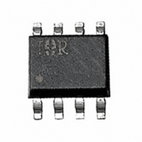
IRF7807VD2PBF International Rectifier, IRF7807VD2PBF Datasheet - Page 4

IRF7807VD2PBF
Manufacturer Part Number
IRF7807VD2PBF
Description
MOSFET N-CH 30V 8.3A 8-SOIC
Manufacturer
International Rectifier
Series
FETKY™r
Datasheet
1.IRF7807VD2TRPBF.pdf
(9 pages)
Specifications of IRF7807VD2PBF
Fet Type
MOSFET N-Channel, Metal Oxide
Fet Feature
Diode (Isolated)
Rds On (max) @ Id, Vgs
25 mOhm @ 7A, 4.5V
Drain To Source Voltage (vdss)
30V
Current - Continuous Drain (id) @ 25° C
8.3A
Vgs(th) (max) @ Id
1V @ 250µA
Gate Charge (qg) @ Vgs
14nC @ 4.5V
Power - Max
2.5W
Mounting Type
Surface Mount
Package / Case
8-SOIC (3.9mm Width)
Lead Free Status / RoHS Status
Lead free / RoHS Compliant
IRF7807VD2PbF
portant characteristic; however, once again the im-
portance of gate charge must not be overlooked since
it impacts three critical areas. Under light load the
MOSFET must still be turned on and off by the con-
trol IC so the gate drive losses become much more
significant. Secondly, the output charge Q
verse recovery charge Q
are transfered to Q1 and increase the dissipation in
that device. Thirdly, gate charge will impact the
MOSFETs’ susceptibility to Cdv/dt turn on.
of the converter and therefore sees transitions be-
tween ground and V
a rate of change of drain voltage dV/dt which is ca-
pacitively coupled to the gate of Q2 and can induce
a voltage spike on the gate that is sufficient to turn
Typical Mobile PC Application
in circuit and correlates well with performance predic-
tions generated by the system models. An advantage of
this new technology platform is that the MOSFETs it
produces are suitable for both control FET and synchro-
nous FET applications. This has been demonstrated with
the 3.3V and 5V converters. (Fig 3 and Fig 4). In these
applications the same MOSFET IRF7807V was used for
both the control FET (Q1) and the synchronous FET
(Q2). This provides a highly effective cost/performance
solution.
93
92
91
90
89
88
87
86
85
84
83
For the synchronous MOSFET Q2, R
The drain of Q2 is connected to the switching node
4
The performance of these new devices has been tested
1
2
in
. As Q1 turns on and off there is
Vin=24V
Vin=14V
Vin=10V
Load current (A)
rr
Figure 3
both generate losses that
3
4
ds(on)
oss
is an im-
and re-
5
the MOSFET on, resulting in shoot-through current .
The ratio of Q
potential for Cdv/dt turn on.
machine readable format at www.irf.com.
Figure 2: Q
95
94
93
92
91
90
89
88
87
86
Spice model for IRF7807V can be downloaded in
1
oss
Characteristic
gd
/Q
2
gs1
must be minimized to reduce the
Load current (A)
Figure 4
3
Vin=24V
Vin=14V
Vin=10V
www.irf.com
4
5


