IRF6709S2TRPBF International Rectifier, IRF6709S2TRPBF Datasheet - Page 2
IRF6709S2TRPBF
Manufacturer Part Number
IRF6709S2TRPBF
Description
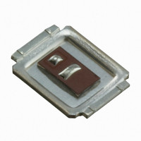
MOSFET N-CH 25V 12A DIRECTFET-S1
Manufacturer
International Rectifier
Series
HEXFET®r
Datasheet
1.IRF6709S2TRPBF.pdf
(10 pages)
Specifications of IRF6709S2TRPBF
Fet Type
MOSFET N-Channel, Metal Oxide
Fet Feature
Logic Level Gate
Rds On (max) @ Id, Vgs
3.8 mOhm @ 19A, 10V
Drain To Source Voltage (vdss)
25V
Current - Continuous Drain (id) @ 25° C
19A
Vgs(th) (max) @ Id
2.35V @ 25µA
Gate Charge (qg) @ Vgs
20nC @ 4.5V
Input Capacitance (ciss) @ Vds
1810pF @ 13V
Power - Max
2.2W
Mounting Type
Surface Mount
Package / Case
DirectFET™ Isometric S1
Transistor Polarity
N-Channel
Resistance Drain-source Rds (on)
13.5 mOhms
Drain-source Breakdown Voltage
25 V
Gate-source Breakdown Voltage
20 V
Continuous Drain Current
39 A
Power Dissipation
21 W
Gate Charge Qg
8.1 nC
Lead Free Status / RoHS Status
Lead free / RoHS Compliant
Available stocks
Company
Part Number
Manufacturer
Quantity
Price

Part Number:
IRF6709S2TRPBF
Manufacturer:
IR
Quantity:
20 000


…
‡
Notes:
BV
∆ΒV
R
V
∆V
I
I
gfs
Q
Q
Q
R
t
t
t
t
C
C
C
I
I
V
t
Q
Static @ T
Diode Characteristics
DSS
GSS
d(on)
r
d(off)
f
S
SM
rr
DS(on)
GS(th)
G
iss
oss
rss
SD
g
Q
Q
Q
Q
sw
oss
rr
Repetitive rating; pulse width limited by max. junction temperature.
Pulse width ≤ 400µs; duty cycle ≤ 2%.
2
GS(th)
DSS
gs1
gs2
gd
godr
DSS
/∆T
/∆T
J
J
J
= 25°C (unless otherwise specified)
Drain-to-Source Breakdown Voltage
Breakdown Voltage Temp. Coefficient
Static Drain-to-Source On-Resistance
Gate Threshold Voltage
Gate Threshold Voltage Coefficient
Drain-to-Source Leakage Current
Gate-to-Source Forward Leakage
Gate-to-Source Reverse Leakage
Forward Transconductance
Total Gate Charge
Pre-Vth Gate-to-Source Charge
Post-Vth Gate-to-Source Charge
Gate-to-Drain Charge
Gate Charge Overdrive
Switch Charge (Q
Output Charge
Gate Resistance
Turn-On Delay Time
Rise Time
Turn-Off Delay Time
Fall Time
Input Capacitance
Output Capacitance
Reverse Transfer Capacitance
Continuous Source Current
(Body Diode)
Pulsed Source Current
(Body Diode)
Diode Forward Voltage
Reverse Recovery Time
Reverse Recovery Charge
Parameter
Parameter
g
gs2
+ Q
gd
)
Min. Typ. Max. Units
Min. Typ. Max. Units
1.35
–––
–––
–––
–––
–––
–––
–––
–––
–––
–––
–––
–––
–––
–––
–––
–––
–––
–––
–––
–––
–––
–––
–––
–––
–––
–––
–––
–––
25
19
1010
10.1
–––
-7.2
–––
–––
–––
–––
–––
340
140
–––
–––
–––
5.9
1.8
8.1
1.9
1.1
2.8
2.3
3.9
4.6
3.2
8.4
9.1
9.5
9.3
19
25
15
-100
13.5
2.35
–––
–––
–––
150
100
–––
–––
–––
–––
–––
–––
–––
–––
–––
–––
–––
–––
–––
–––
–––
100
7.8
1.0
1.0
12
26
23
14
mV/°C
mV/°C
mΩ
µA
nA
nC
nC
nC
pF
ns
ns
Ω
V
V
S
A
V
See Fig. 18
V
Reference to 25°C, I
V
V
V
V
V
V
V
V
V
V
I
V
V
I
R
V
V
ƒ = 1.0MHz
MOSFET symbol
showing the
integral reverse
p-n junction diode.
T
T
di/dt = 200A/µs
D
D
J
J
GS
GS
GS
DS
DS
DS
GS
GS
DS
DS
GS
DS
DD
GS
DS
G
= 10A
= 10A
= 6.2Ω
= 25°C, I
= 25°C, I
= V
= 20V, V
= 20V, V
= 13V, I
= 13V
= 10V, V
= 13V
= 0V, I
= 10V, I
= 4.5V, I
= 20V
= -20V
= 4.5V
= 13V, V
= 0V
GS
, I
D
Conditions
D
Conditions
S
F
D
D
= 250µA
D
GS
GS
GS
GS
= 10A, V
=10A
= 25µA
=10A
= 12A
= 10A
= 0V
= 0V, T
= 0V
= 4.5V
i
D
i
i
www.irf.com
GS
= 1mA
J
= 125°C
i
= 0V
i
Related parts for IRF6709S2TRPBF
Image
Part Number
Description
Manufacturer
Datasheet
Request
R

Part Number:
Description:
SCHOTTKY RECTIFIER
Manufacturer:
International Rectifier Corp.
Datasheet:
Part Number:
Description:
SCHOTTKY RECTIFIER
Manufacturer:
International Rectifier Corp.
Datasheet:
Part Number:
Description:
SCHOTTKY RECTIFIER
Manufacturer:
International Rectifier Corp.
Datasheet:
Part Number:
Description:
SCHOTTKY RECTIFIER
Manufacturer:
International Rectifier Corp.
Datasheet:
Part Number:
Description:
SCHOTTKY RECTIFIER
Manufacturer:
International Rectifier Corp.
Datasheet:
Part Number:
Description:
SCHOTTKY RECTIFIER
Manufacturer:
International Rectifier Corp.
Datasheet:
Part Number:
Description:
SCHOTTKY RECTIFIER
Manufacturer:
International Rectifier Corp.
Datasheet:
Part Number:
Description:
SCHOTTKY RECTIFIER
Manufacturer:
International Rectifier Corp.
Datasheet:
Part Number:
Description:
SCHOTTKY RECTIFIER
Manufacturer:
International Rectifier Corp.
Datasheet:
Part Number:
Description:
SCHOTTKY RECTIFIER
Manufacturer:
International Rectifier Corp.
Datasheet:
Part Number:
Description:
SCHOTTKY RECTIFIER
Manufacturer:
International Rectifier Corp.
Datasheet:
Part Number:
Description:
SCHOTTKY RECTIFIER
Manufacturer:
International Rectifier Corp.
Datasheet:
Part Number:
Description:
SCHOTTKY RECTIFIER
Manufacturer:
International Rectifier Corp.
Datasheet:
Part Number:
Description:
SCHOTTKY RECTIFIER
Manufacturer:
International Rectifier Corp.
Datasheet:
Part Number:
Description:
SCHOTTKY RECTIFIER
Manufacturer:
International Rectifier Corp.
Datasheet: