IRFB4019PBF International Rectifier, IRFB4019PBF Datasheet
IRFB4019PBF
Specifications of IRFB4019PBF
Available stocks


Related parts for IRFB4019PBF

IRFB4019PBF Summary of contents
Page 1
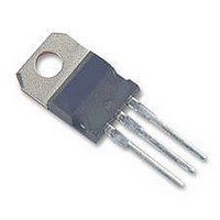
... Junction-to-Ambient f R θJA Notes through … are on page 2 www.irf.com Key Parameters typ. @ 10V DS(ON) Q typ typ typ. G(int) T max Gate Parameter @ 10V GS @ 10V GS Parameter IRFB4019PbF 150 5.1 nC Ω 2.4 175 ° TO-220AB D S Drain Source Max. Units 150 V ± ...
Page 2
Electrical Characteristics @ T Parameter BV Drain-to-Source Breakdown Voltage DSS ∆ΒV /∆T Breakdown Voltage Temp. Coefficient DSS J R Static Drain-to-Source On-Resistance DS(on) V Gate Threshold Voltage GS(th) ∆V /∆T Gate Threshold Voltage Coefficient GS(th Drain-to-Source Leakage Current ...
Page 3
TOP 10 BOTTOM 1 0.1 5.0V ≤ 60µs PULSE WIDTH Tj = 25°C 0.01 0 Drain-to-Source Voltage (V) Fig 1. Typical Output Characteristics 100 25V ≤ 60µs PULSE WIDTH 10.0 T ...
Page 4
175° 25°C 0.1 0.0 0.5 1 Source-to-Drain Voltage (V) Fig 7. Typical Source-Drain Diode Forward Voltage 100 125 T ...
Page 5
125°C 0 25°C 0 Gate-to-Source Voltage (V) Fig 12. On-Resistance Vs. Gate Voltage 100 Duty Cycle = Single Pulse 10 0.01 0.05 ...
Page 6
D.U.T + ƒ • • - • + ‚ - • • • SD • Fig 16 D.U 20V V GS 0.01 Ω Fig 17a. Unclamped Inductive Test Circuit V ...
Page 7
EXAMPLE: T HIS IS AN IRF1010 LOT CODE 1789 AS SEMBLED ON WW 19, 2000 EMBLY LINE "C" Note: "P" embly line pos ition indicates "Lead - Free" TO-220AB packages are not ...
Page 8
Note: For the most current drawings please refer to the IR website at: http://www.irf.com/package/ ...