IRF6633TR1 International Rectifier, IRF6633TR1 Datasheet
IRF6633TR1
Specifications of IRF6633TR1
Available stocks


Related parts for IRF6633TR1


IRF6633TR1 Summary of contents
Page 1
RoHs Compliant Containing No Lead and Bromide l Low Profile (<0.7 mm) l Dual Sided Cooling Compatible l Ultra Low Package Inductance l Optimized for High Frequency Switching l Ideal for CPU Core DC-DC Converters l Optimized ...
Page 2
IRF6633 Static @ T = 25°C (unless otherwise specified) J Parameter BV Drain-to-Source Breakdown Voltage DSS ∆ΒV /∆T Breakdown Voltage Temp. Coefficient DSS J R Static Drain-to-Source On-Resistance DS(on) V Gate Threshold Voltage GS(th) ∆V /∆T Gate Threshold Voltage Coefficient ...
Page 3
Absolute Maximum Ratings 25°C Power Dissipation D A Power Dissipation 70° 25°C Power Dissipation Peak Soldering Temperature P T Operating Junction and J T Storage Temperature ...
Page 4
IRF6633 1000 100 10 1 2.5V ≤60µs PULSE WIDTH Tj = 25°C 0.1 0 Drain-to-Source Voltage (V) Fig 4. Typical Output Characteristics 1000 100 150° 25° -40°C ...
Page 5
150°C 100 25° -40°C 10.0 1.0 0.1 0.2 0.4 0.6 0 Source-to-Drain Voltage (V) Fig 10. Typical Source-Drain Diode Forward Voltage ...
Page 6
IRF6633 0 1K Fig 15a. Gate Charge Test Circuit D.U 20V 0.01 Ω Fig 16a. Unclamped Inductive Test Circuit Pulse Width < 1µs Duty Factor < ...
Page 7
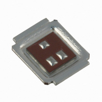
D.U.T + ƒ • • - • + ‚ - R • • • SD • Fig 18. DirectFET™ Substrate and PCB Layout, MP Outline (Medium Size Can, P-Designation). Please see DirectFET application note AN-1035 for all details regarding ...
Page 8
IRF6633 DirectFET™ Outline Dimension, MP Outline (Medium Size Can, P-Designation). Please see DirectFET application note AN-1035 for all details regarding the assembly of DirectFET. This includes all recommendations for stencil and substrate designs. DirectFET™ Part Marking 8 DIMENSIONS IMPERIAL METRIC ...
Page 9
... DirectFET™ Tape & Reel Dimension (Showing component orientation). NOTE: Controlling dimensions in mm Std reel quantity is 4800 parts. (ordered as IRF6633). For 1000 parts on 7" reel, order IRF6633TR1 CODE WORLD HEADQUARTERS: 233 Kansas St., El Segundo, California 90245, USA Tel: (310) 252-7105 www.irf.com ...
Page 10
Note: For the most current drawings please refer to the IR website at: http://www.irf.com/package/ ...