IRFS4321TRLPBF International Rectifier, IRFS4321TRLPBF Datasheet - Page 2
IRFS4321TRLPBF
Manufacturer Part Number
IRFS4321TRLPBF
Description
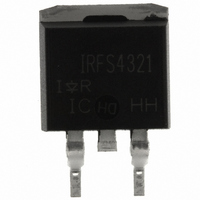
MOSFET N-CH 150V 83A D2PAK
Manufacturer
International Rectifier
Series
HEXFET®r
Datasheet
1.IRFSL4321PBF.pdf
(10 pages)
Specifications of IRFS4321TRLPBF
Fet Type
MOSFET N-Channel, Metal Oxide
Fet Feature
Standard
Rds On (max) @ Id, Vgs
15 mOhm @ 33A, 10V
Drain To Source Voltage (vdss)
150V
Current - Continuous Drain (id) @ 25° C
83A
Vgs(th) (max) @ Id
5V @ 250µA
Gate Charge (qg) @ Vgs
110nC @ 10V
Input Capacitance (ciss) @ Vds
4460pF @ 25V
Power - Max
330W
Mounting Type
Surface Mount
Package / Case
D²Pak, TO-263 (2 leads + tab)
Transistor Polarity
N Channel
Continuous Drain Current Id
85A
Drain Source Voltage Vds
100V
On Resistance Rds(on)
12mohm
Rds(on) Test Voltage Vgs
10V
Threshold Voltage Vgs Typ
5V
Rohs Compliant
Yes
Lead Free Status / RoHS Status
Lead free / RoHS Compliant
Other names
IRFS4321TRLPBFTR
Available stocks
Company
Part Number
Manufacturer
Quantity
Price
Company:

Part Number:
IRFS4321TRLPBF
Manufacturer:
Opto Diod
Quantity:
20
Part Number:
IRFS4321TRLPBF
Manufacturer:
INFINEON/英飞凌
Quantity:
20 000


Notes:
‚
ƒ
Static @ T
V
R
V
I
I
R
Dynamic @ T
gfs
Q
Q
Q
t
t
t
t
C
C
C
Diode Characteristics
I
I
V
t
Q
I
t
DSS
GSS
d(on)
r
d(off)
f
S
SM
rr
RRM
on
V
(BR)DSS
GS(th)
SD
DS(on)
G(int)
iss
oss
rss
g
gs
gd
rr
temperature. Package limitation current is 75A
above this value.
2
Calculated continuous current based on maximum allowable junction
Repetitive rating; pulse width limited by max. junction
Limited by T
temperature.
Symbol
Symbol
Symbol
R
(BR)DSS
G
= 25 , I
/ T
J
AS
Jmax
J
Drain-to-Source Breakdown Voltage
Breakdown Voltage Temp. Coefficient
Static Drain-to-Source On-Resistance
Gate Threshold Voltage
Drain-to-Source Leakage Current
Gate-to-Source Forward Leakage
Gate-to-Source Reverse Leakage
Internal Gate Resistance
Forward Transconductance
Total Gate Charge
Gate-to-Source Charge
Gate-to-Drain ("Miller") Charge
Turn-On Delay Time
Rise Time
Turn-Off Delay Time
Fall Time
Input Capacitance
Output Capacitance
Reverse Transfer Capacitance
Continuous Source Current
(Body Diode)
Pulsed Source Current
(Body Diode)
Diode Forward Voltage
Reverse Recovery Time
Reverse Recovery Charge
Reverse Recovery Current
Forward Turn-On Time
= 25°C (unless otherwise specified)
= 50A, V
, starting T
J
= 25°C (unless otherwise specified)
Parameter
GS
=10V. Part not recommended for use
J
= 25°C, L = 0.096mH
Ãd
Parameter
Parameter
Intrinsic turn-on time is negligible (turn-on is dominated by LS+LD)
Min. Typ. Max. Units
Min. Typ. Max. Units
Min. Typ. Max. Units
150
–––
–––
–––
–––
–––
–––
–––
130
–––
–––
–––
–––
–––
–––
–––
–––
–––
–––
–––
–––
–––
–––
–––
–––
3.0
„
…
4460
–––
150
–––
–––
–––
–––
–––
–––
390
–––
–––
–––
300
0.8
6.5
12
60
89
71
24
21
18
25
35
82
Pulse width
-100
85
–––
––– mV/°C
100
–––
–––
110
–––
–––
–––
–––
–––
–––
–––
–––
–––
330
130
450
–––
5.0
1.0
1.3
15
20
400μs; duty cycle
m
mA
μA
nA
nC
nC
ns
pF
ns
S
A
V
V
V
A
A
V
Reference to 25°C, I
V
V
V
V
V
V
V
I
V
V
V
I
R
V
V
V
ƒ = 1.0MHz
MOSFET symbol
showing the
integral reverse
p-n junction diode.
T
I
V
di/dt = 100A/μs
D
D
D
J
GS
GS
DS
DS
DS
GS
GS
DS
DS
GS
DD
G
GS
GS
DS
R
= 50A
= 50A
= 50A
= 25°C, I
= 128V,
= 2.5
= V
= 150V, V
= 150V, V
= 25V, I
= 75V
= 50V
= 0V, I
= 10V, I
= 20V
= -20V
= 10V
= 98V
= 10V
= 0V
GS
, I
D
f
f
2%.
D
S
D
D
= 250μA
= 50A, V
= 250μA
= 50A
= 33A
GS
GS
Conditions
Conditions
Conditions
f
= 0V
= 0V, T
D
f
GS
= 1mA
J
= 0V
= 125°C
d
www.irf.com
f
G
D
S
Related parts for IRFS4321TRLPBF
Image
Part Number
Description
Manufacturer
Datasheet
Request
R

Part Number:
Description:
SCHOTTKY RECTIFIER
Manufacturer:
International Rectifier Corp.
Datasheet:
Part Number:
Description:
SCHOTTKY RECTIFIER
Manufacturer:
International Rectifier Corp.
Datasheet:
Part Number:
Description:
SCHOTTKY RECTIFIER
Manufacturer:
International Rectifier Corp.
Datasheet:
Part Number:
Description:
SCHOTTKY RECTIFIER
Manufacturer:
International Rectifier Corp.
Datasheet:
Part Number:
Description:
SCHOTTKY RECTIFIER
Manufacturer:
International Rectifier Corp.
Datasheet:
Part Number:
Description:
SCHOTTKY RECTIFIER
Manufacturer:
International Rectifier Corp.
Datasheet:
Part Number:
Description:
SCHOTTKY RECTIFIER
Manufacturer:
International Rectifier Corp.
Datasheet:
Part Number:
Description:
SCHOTTKY RECTIFIER
Manufacturer:
International Rectifier Corp.
Datasheet:
Part Number:
Description:
SCHOTTKY RECTIFIER
Manufacturer:
International Rectifier Corp.
Datasheet:
Part Number:
Description:
SCHOTTKY RECTIFIER
Manufacturer:
International Rectifier Corp.
Datasheet:
Part Number:
Description:
SCHOTTKY RECTIFIER
Manufacturer:
International Rectifier Corp.
Datasheet:
Part Number:
Description:
SCHOTTKY RECTIFIER
Manufacturer:
International Rectifier Corp.
Datasheet:
Part Number:
Description:
SCHOTTKY RECTIFIER
Manufacturer:
International Rectifier Corp.
Datasheet:
Part Number:
Description:
SCHOTTKY RECTIFIER
Manufacturer:
International Rectifier Corp.
Datasheet:
Part Number:
Description:
SCHOTTKY RECTIFIER
Manufacturer:
International Rectifier Corp.
Datasheet: