IRFPS3810PBF International Rectifier, IRFPS3810PBF Datasheet - Page 2
IRFPS3810PBF
Manufacturer Part Number
IRFPS3810PBF
Description
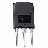
MOSFET N-CH 100V 170A SUPER247
Manufacturer
International Rectifier
Series
HEXFET®r
Specifications of IRFPS3810PBF
Fet Type
MOSFET N-Channel, Metal Oxide
Fet Feature
Standard
Rds On (max) @ Id, Vgs
9 mOhm @ 100A, 10V
Drain To Source Voltage (vdss)
100V
Current - Continuous Drain (id) @ 25° C
170A
Vgs(th) (max) @ Id
5V @ 250µA
Gate Charge (qg) @ Vgs
390nC @ 10V
Input Capacitance (ciss) @ Vds
6790pF @ 25V
Power - Max
580W
Mounting Type
Through Hole
Package / Case
Super-247-3 (Straight Leads)
Current, Drain
170 A
Gate Charge, Total
260 nC
Package Type
Super-247™
Polarization
N-Channel
Power Dissipation
580 W
Resistance, Drain To Source On
0.009 Ohm
Temperature, Operating, Maximum
+175 °C
Temperature, Operating, Minimum
-55 °C
Time, Turn-off Delay
45 ns
Time, Turn-on Delay
24 ns
Transconductance, Forward
52 S
Voltage, Breakdown, Drain To Source
100 V
Voltage, Forward, Diode
1.3 V
Voltage, Gate To Source
±30 V
Configuration
Single
Transistor Polarity
N-Channel
Resistance Drain-source Rds (on)
9 m Ohms
Drain-source Breakdown Voltage
100 V
Gate-source Breakdown Voltage
30 V
Continuous Drain Current
141 A
Maximum Operating Temperature
+ 175 C
Mounting Style
Through Hole
Fall Time
140 ns
Gate Charge Qg
260 nC
Minimum Operating Temperature
- 55 C
Rise Time
270 ns
Lead Free Status / RoHS Status
Lead free / RoHS Compliant
Other names
*IRFPS3810PBF
Available stocks
Company
Part Number
Manufacturer
Quantity
Price
Company:

Part Number:
IRFPS3810PBF
Manufacturer:
IR
Quantity:
5 203
Part Number:
IRFPS3810PBF
Manufacturer:
IR
Quantity:
20 000


Electrical Characteristics @ T
Source-Drain Ratings and Characteristics
‚
ƒ
Notes:
I
I
V
∆V
R
V
g
Q
Q
Q
t
t
t
t
C
C
C
C
C
C
L
L
I
I
V
t
Q
t
DSS
GSS
SM
d(on)
r
d(off)
f
S
rr
on
2
fs
D
S
(BR)DSS
DS(on)
GS(th)
iss
oss
rss
oss
oss
oss
SD
g
gs
gd
rr
Repetitive rating; pulse width limited by
I
(BR)DSS
R
max. junction temperature. (See fig. 11)
T
Starting T
SD
J
G
eff.
≤ 175°C
≤ 100A, di/dt ≤ 350A/µs, V
= 25Ω, I
/∆T
J
J
Drain-to-Source Leakage Current
Effective Output Capacitance …
Drain-to-Source Breakdown Voltage
Breakdown Voltage Temp. Coefficient
Static Drain-to-Source On-Resistance
Gate Threshold Voltage
Forward Transconductance
Gate-to-Source Forward Leakage
Gate-to-Source Reverse Leakage
Total Gate Charge
Gate-to-Source Charge
Gate-to-Drain ("Miller") Charge
Turn-On Delay Time
Rise Time
Turn-Off Delay Time
Fall Time
Internal Drain Inductance
Internal Source Inductance
Input Capacitance
Output Capacitance
Reverse Transfer Capacitance
Output Capacitance
Output Capacitance
Continuous Source Current
(Body Diode)
Pulsed Source Current
(Body Diode)
Diode Forward Voltage
Reverse Recovery Time
Reverse RecoveryCharge
Forward Turn-On Time
= 25°C, L = 0.27mH
AS
= 100A. (See Figure 12)
Parameter
Parameter
DD
≤ V
(BR)DSS
J
= 25°C (unless otherwise specified)
,
…
†
„
C
Pulse width ≤ 400µs; duty cycle ≤ 2%.
as C
100
–––
–––
–––
–––
–––
–––
–––
–––
–––
–––
–––
–––
–––
–––
–––
–––
–––
–––
–––
––– 10740 –––
Min. Typ. Max. Units
3.0
Min. Typ. Max. Units
oss
Calculated continuous current based on maximum allowable
52
–––
–––
–––
–––
–––
––– 1640 2460
junction temperature. Package limitation current is 105A.
Intrinsic turn-on time is negligible (turn-on is dominated by L
eff. is a fixed capacitance that gives the same charging time
oss
6790 –––
2470 –––
1180 –––
2210 –––
0.11 –––
while V
–––
––– 0.009
–––
–––
–––
–––
–––
––– -100
260
160
270
140
990
–––
–––
–––
220
5.0
49
24
45
13
170†
–––
–––
–––
250
100
390
250
–––
–––
–––
–––
–––
–––
330
5.0
1.3
25
74
DS
670
is rising from 0 to 80% V
V/°C
nH
µA
nA
nC
ns
nC
pF
ns
Ω
V
V
S
V
V
Reference to 25°C, I
V
V
V
V
V
V
V
I
V
V
V
I
R
V
Between lead,
6mm (0.25in.)
from package
and center of die contact
V
V
ƒ = 1.0MHz, See Fig. 5
V
V
V
MOSFET symbol
showing the
integral reverse
p-n junction diode.
T
T
di/dt = 100A/µs „
D
D
J
J
GS
GS
DS
DS
DS
DS
GS
GS
DS
GS
DD
GS
GS
DS
GS
GS
GS
G
= 100A
= 100A
= 25°C, I
= 25°C, I
= 1.03Ω
= 0V, I
= 10V, I
= 10V, I
= 50V, I
= 100V, V
= 80V, V
= 30V
= -30V
= 80V
= 10V„
= 50V
= 10V „
= 0V
= 25V
= 0V, V
= 0V, V
= 0V, V
D
S
F
DS
D
D
D
DS
DS
Conditions
= 250µA
GS
Conditions
= 100A, V
= 100A
DSS
= 250µA
= 100A
= 100A „
GS
= 0V to 80V
= 1.0V, ƒ = 1.0MHz
= 80V, ƒ = 1.0MHz
= 0V, T
= 0V
www.irf.com
D
= 1mA
GS
J
= 150°C
G
= 0V „
G
S
+L
D
D
S
)
S
D
Related parts for IRFPS3810PBF
Image
Part Number
Description
Manufacturer
Datasheet
Request
R

Part Number:
Description:
SCHOTTKY RECTIFIER
Manufacturer:
International Rectifier Corp.
Datasheet:
Part Number:
Description:
SCHOTTKY RECTIFIER
Manufacturer:
International Rectifier Corp.
Datasheet:
Part Number:
Description:
SCHOTTKY RECTIFIER
Manufacturer:
International Rectifier Corp.
Datasheet:
Part Number:
Description:
SCHOTTKY RECTIFIER
Manufacturer:
International Rectifier Corp.
Datasheet:
Part Number:
Description:
SCHOTTKY RECTIFIER
Manufacturer:
International Rectifier Corp.
Datasheet:
Part Number:
Description:
SCHOTTKY RECTIFIER
Manufacturer:
International Rectifier Corp.
Datasheet:
Part Number:
Description:
SCHOTTKY RECTIFIER
Manufacturer:
International Rectifier Corp.
Datasheet:
Part Number:
Description:
SCHOTTKY RECTIFIER
Manufacturer:
International Rectifier Corp.
Datasheet:
Part Number:
Description:
SCHOTTKY RECTIFIER
Manufacturer:
International Rectifier Corp.
Datasheet:
Part Number:
Description:
SCHOTTKY RECTIFIER
Manufacturer:
International Rectifier Corp.
Datasheet:
Part Number:
Description:
SCHOTTKY RECTIFIER
Manufacturer:
International Rectifier Corp.
Datasheet:
Part Number:
Description:
SCHOTTKY RECTIFIER
Manufacturer:
International Rectifier Corp.
Datasheet:
Part Number:
Description:
SCHOTTKY RECTIFIER
Manufacturer:
International Rectifier Corp.
Datasheet:
Part Number:
Description:
SCHOTTKY RECTIFIER
Manufacturer:
International Rectifier Corp.
Datasheet:
Part Number:
Description:
SCHOTTKY RECTIFIER
Manufacturer:
International Rectifier Corp.
Datasheet: