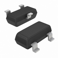
NTR4171PT1G ON Semiconductor, NTR4171PT1G Datasheet - Page 2

NTR4171PT1G
Manufacturer Part Number
NTR4171PT1G
Description
MOSFET P-CH 30V 2.2A SOT23
Manufacturer
ON Semiconductor
Datasheet
1.NTR4171PT3G.pdf
(6 pages)
Specifications of NTR4171PT1G
Fet Type
MOSFET P-Channel, Metal Oxide
Fet Feature
Logic Level Gate
Rds On (max) @ Id, Vgs
75 mOhm @ 2.2A, 10V
Drain To Source Voltage (vdss)
30V
Current - Continuous Drain (id) @ 25° C
2.2A
Vgs(th) (max) @ Id
1.4V @ 250µA
Gate Charge (qg) @ Vgs
15.6nC @ 10V
Input Capacitance (ciss) @ Vds
720pF @ 15V
Power - Max
480mW
Mounting Type
Surface Mount
Package / Case
SOT-23-3, TO-236-3, Micro3™, SSD3, SST3
Configuration
Single
Transistor Polarity
P-Channel
Resistance Drain-source Rds (on)
0.075 Ohm @ 10 V
Forward Transconductance Gfs (max / Min)
7 S
Drain-source Breakdown Voltage
30 V
Gate-source Breakdown Voltage
+/- 12 V
Continuous Drain Current
3.5 A
Power Dissipation
1250 mW
Maximum Operating Temperature
+ 150 C
Mounting Style
SMD/SMT
Minimum Operating Temperature
- 55 C
Lead Free Status / RoHS Status
Lead free / RoHS Compliant
Available stocks
Company
Part Number
Manufacturer
Quantity
Price
Company:
Part Number:
NTR4171PT1G
Manufacturer:
ON Semiconductor
Quantity:
40 075
Company:
Part Number:
NTR4171PT1G
Manufacturer:
ON
Quantity:
30 000
Part Number:
NTR4171PT1G
Manufacturer:
ON/安森美
Quantity:
20 000
2. Surface−mounted on FR4 board using 1 in sq pad size (Cu area = 1.127 in sq [2 oz] including traces)
3. Pulse Test: Pulse Width v 300 ms, Duty Cycle v 2%
4. Switching characteristics are independent of operating junction temperatures
MOSFET ELECTRICAL CHARACTERISTICS
OFF CHARACTERISTICS
ON CHARACTERISTICS (Note 3)
CHARGES, CAPACITANCES AND GATE RESISTANCE
SWITCHING CHARACTERISTICS, V
DRAIN−SOURCE DIODE CHARACTERISTICS
Drain−to−Source Breakdown Voltage
Drain−to−Source Breakdown Voltage
Temperature Coefficient
Zero Gate Voltage Drain Current
Gate−to−Source Leakage Current
Gate Threshold Voltage
Negative Threshold Temperature Coefficient
Drain−to−Source On−Resistance
Forward Transconductance
Input Capacitance
Output Capacitance
Reverse Transfer Capacitance
Total Gate Charge
Threshold Gate Charge
Gate−to−Source Charge
Gate−to−Drain Charge
Total Gate Charge
Threshold Gate Charge
Gate−to−Source Charge
Gate−to−Drain Charge
Gate Resistance
Turn−On Delay Time
Rise Time
Turn−Off Delay Time
Fall Time
Turn−On Delay Time
Rise Time
Turn−Off Delay Time
Fall Time
Forward Diode Voltage
Reverse Recovery Time
Charge Time
Discharge Time
Reverse Recovery Charge
Parameter
GS
= 4.5 V (Note 4)
V
V
V
Symbol
V
Q
Q
GS(TH)
R
Q
Q
(BR)DSS
(BR)DSS
GS(TH)
t
t
t
t
I
C
G(TOT)
Q
G(TOT)
Q
I
DS(on)
Q
Q
Q
C
C
V
g
d(on)
d(off)
d(on)
d(off)
DSS
GSS
G(TH)
G(TH)
t
/T
R
RR
t
t
oss
t
t
t
t
FS
rss
GS
GD
GS
GD
SD
RR
iss
a
b
G
r
f
r
f
J
(T
/T
J
J
= 25°C unless otherwise noted)
http://onsemi.com
V
V
V
I
D
GS
GS
GS
= −250 mA, Reference to 25°C
V
V
V
V
= 0 V, V
= 0 V, V
V
V
V
V
V
V
GS
GS
GS
GS
V
= 0 V, I
V
V
GS
GS
2
GS
DS
DS
GS
I
I
GS
GS
D
D
GS
= −4.5 V, V
= −4.5 V, V
dI
= −10 V, V
= −10 V, V
= −3.5 A, R
= −3.5 A, R
Test Condition
= −4.5 V, I
= −2.5 V, I
= −5.0 V, I
= 0 V, V
= V
= −10 V, I
= 0 V, I
SD
= 0 V, f = 1.0 MHz,
= 0 V, I
V
I
I
D
D
S
DS
DS
DS
/d
DS
= −1.0 A, T
= −3.5 A
= −3.5 A
t
= −24 V, T
= −24 V, T
, I
= −15 V
= 100 A/ms
D
GS
D
S
= −250 mA
DS
DS
DS
DS
= −1.0 A,
= −250 mA
D
D
D
D
G
G
= "12 V
= −2.2 A
= −1.8 A
= −2.2 A
= −1.0 A
= −15 V,
= −15 V,
= −15 V,
= −15 V,
= 6 W
= 6 W
J
J
J
= 25°C
= 25°C
= 85°C
−0.7
Min
−30
−1.15
15.6
−0.8
Typ
720
3.5
7.0
0.7
1.6
2.6
7.4
0.7
1.6
2.6
6.1
8.0
9.0
4.0
8.0
24
50
60
90
95
65
32
14
16
25
22
14
10
11
Max
−1.0
−5.0
±0.1
−1.4
−1.2
150
110
75
mV/°C
mV/°C
Units
mW
nC
nC
nC
mA
mA
pF
ns
ns
ns
W
V
V
S
V


