NTGS3441T1G ON Semiconductor, NTGS3441T1G Datasheet
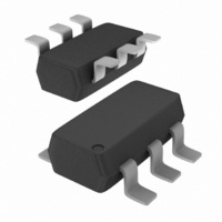
MOSFET P-CH 20V 1.65A 6-TSOP

NTGS3441T1G

Manufacturer Part Number
NTGS3441T1G
Description
MOSFET P-CH 20V 1.65A 6-TSOP
Manufacturer
ON Semiconductor
Datasheet

Specifications of NTGS3441T1G

Fet Type
MOSFET P-Channel, Metal Oxide
Fet Feature
Logic Level Gate
Rds On (max) @ Id, Vgs
90 mOhm @ 3.3A, 4.5V
Drain To Source Voltage (vdss)
20V
Current - Continuous Drain (id) @ 25° C
1.65A
Vgs(th) (max) @ Id
1.5V @ 250µA
Gate Charge (qg) @ Vgs
14nC @ 4.5V
Input Capacitance (ciss) @ Vds
480pF @ 5V
Power - Max
500mW
Mounting Type
Surface Mount
Package / Case
SC-74-6
Configuration
Single Quad Drain
Transistor Polarity
P-Channel
Resistance Drain-source Rds (on)
0.09 Ohm @ 4.5 V
Forward Transconductance Gfs (max / Min)
6.8 S
Drain-source Breakdown Voltage
20 V
Gate-source Breakdown Voltage
+/- 8 V
Continuous Drain Current
3.3 A
Power Dissipation
2000 mW
Maximum Operating Temperature
+ 150 C
Mounting Style
SMD/SMT
Minimum Operating Temperature
- 55 C
Lead Free Status / RoHS Status
Lead free / RoHS Compliant
Other names
NTGS3441T1GOSTR

Available stocks

Company
Part Number
Manufacturer
Quantity
Price
Part Number:
NTGS3441T1G
Manufacturer:
ON
Quantity:
33 000
Part Number:
NTGS3441T1G
Manufacturer:
ON
Quantity:
30 000
Part Number:
NTGS3441T1G
Manufacturer:
ONSemiconduc
Quantity:
2 070
Part Number:
NTGS3441T1G
Manufacturer:
ON/安森美
Quantity:
20 000
NTGS3441T1
Power MOSFET
1 Amp, 20 Volts
P−Channel TSOP−6
Features
Applications
Maximum ratings are those values beyond which device damage can occur.
Maximum ratings applied to the device are individual stress limit values (not
normal operating conditions) and are not valid simultaneously. If these limits are
exceeded, device functional operation is not implied, damage may occur and
reliability may be affected.
1. Minimum FR−4 or G−10 PCB, operating to steady state.
2. Mounted onto a 2″ square FR−4 board (1 in sq, 2 oz. Cu. 0.06″ thick single
3. Mounted onto a 2″ square FR−4 board (1 in sq, 2 oz. Cu. 0.06″ thick single
MAXIMUM RATINGS
© Semiconductor Components Industries, LLC, 2006
February, 2006 − Rev. 5
Drain−to−Source Voltage
Gate−to−Source Voltage − Continuous
Thermal Resistance
Total Power Dissipation @ T
Drain Current − Continuous @ T
Thermal Resistance
Total Power Dissipation @ T
Drain Current − Continuous @ T
Thermal Resistance
Total Power Dissipation @ T
Drain Current − Continuous @ T
Operating and Storage Temperature Range
Maximum Lead Temperature for Soldering
i.e.: Cellular and Cordless Telephones, and PCMCIA Cards
Ultra Low R
Higher Efficiency Extending Battery Life
Miniature TSOP−6 Surface Mount Package
Pb−Free Package is Available
Power Management in Portable and Battery−Powered Products,
sided), operating to steady state.
sided), t t 5.0 seconds.
Junction−to−Ambient (Note 1)
− Pulsed Drain Current (T
Junction−to−Ambient (Note 2)
− Pulsed Drain Current (T
Junction−to−Ambient (Note 3)
− Pulsed Drain Current (T
Purposes for 10 Seconds
DS(on)
Rating
(T
J
= 25°C unless otherwise noted)
A
A
A
p
p
p
= 25°C
= 25°C
= 25°C
t 10 mS)
t 10 mS)
t 10 mS)
A
A
A
= 25°C
= 25°C
= 25°C
Symbol
T
V
R
R
R
J
V
I
I
I
DSS
P
P
P
, T
T
I
DM
I
DM
I
DM
qJA
qJA
qJA
GS
D
D
D
L
d
d
d
stg
−55 to 150
Value
−1.65
−2.35
"8.0
62.5
−3.3
−20
244
−10
128
−14
−20
260
0.5
1.0
2.0
1
°C/W
°C/W
°C/W
Unit
°C
°C
W
W
W
V
V
A
A
A
A
A
A
†For information on tape and reel specifications,
NTGS3441T1
NTGS3441T1G
including part orientation and tape sizes, please
refer to our Tape and Reel Packaging Specifications
Brochure, BRD8011/D.
CASE 318G
*Date Code orientation may vary depending
STYLE 1
upon manufacturing location.
Device
TSOP−6
(Note: Microdot may be in either location)
PT
M
G
ORDERING INFORMATION
1
R
3
http://onsemi.com
DS(on)
= Specific Device Code
= Date Code*
= Pb−Free Package
1 AMPERE
20 VOLTS
(Pb−Free)
Package
TSOP−6
TSOP−6
MARKING DIAGRAM &
P−Channel
4
PIN ASSIGNMENT
= 90 mW
Publication Order Number:
1 2 5 6
Drain
Drain
6
1
PT M G
3000 / Tape & Reel
3000 / Tape& Reel
Drain
Drain
G
5
2
NTGS3441T1/D
Shipping
Source
4
3
Gate

Related parts for NTGS3441T1G

NTGS3441T1G Summary of contents

Page 1

... Microdot may be in either location) T 260 °C L *Date Code orientation may vary depending upon manufacturing location. Device NTGS3441T1 NTGS3441T1G †For information on tape and reel specifications, including part orientation and tape sizes, please refer to our Tape and Reel Packaging Specifications Brochure, BRD8011/D. 1 http://onsemi.com 1 AMPERE 20 VOLTS ...

Page 2

ELECTRICAL CHARACTERISTICS Characteristic OFF CHARACTERISTICS Drain−Source Breakdown Voltage ( Vdc −10 mA Zero Gate Voltage Drain Current ( Vdc −20 Vdc 25° ...

Page 3

TYPICAL ELECTRICAL CHARACTERISTICS 25° − −3 − −4 − −10 ...

Page 4

TYPICAL ELECTRICAL CHARACTERISTICS 1200 iss 900 C rss 600 300 −V − GATE−TO−SOURCE OR DRAIN−TO−SOURCE VOLTAGE (VOLTS) Figure 7. Capacitance Variation ...

Page 5

TYPICAL ELECTRICAL CHARACTERISTICS 0.01 1 Duty Cycle = 0.5 0.2 0.1 0.1 0.05 0.02 0.01 Single Pulse 0.01 1E−04 1E−03 1E−02 Figure 12. Normalized Thermal Transient Impedance, Junction−to−Ambient 0.10 1.00 10.00 TIME (sec) Figure ...

Page 6

... Pb−Free strategy and soldering details, please download the ON Semiconductor Soldering and Mounting Techniques Reference Manual, SOLDERRM/D. ON Semiconductor and are registered trademarks of Semiconductor Components Industries, LLC (SCILLC). SCILLC reserves the right to make changes without further notice to any products herein ...

Related keywords