NTD4963N-1G ON Semiconductor, NTD4963N-1G Datasheet - Page 3
NTD4963N-1G
Manufacturer Part Number
NTD4963N-1G
Description
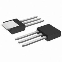
MOSFET N-CH 30V 8.1A IPAK
Manufacturer
ON Semiconductor
Datasheet
1.NTD4963NT4G.pdf
(7 pages)
Specifications of NTD4963N-1G
Package / Case
IPak, TO-251, DPak (3 straight short leads + tab)
Mounting Type
Through Hole
Power - Max
1.1W
Fet Type
MOSFET N-Channel, Metal Oxide
Gate Charge (qg) @ Vgs
16.2nC @ 10V
Vgs(th) (max) @ Id
2.5V @ 250µA
Current - Continuous Drain (id) @ 25° C
8.1A
Drain To Source Voltage (vdss)
30V
Fet Feature
Logic Level Gate
Rds On (max) @ Id, Vgs
9.6 mOhm @ 30A, 10V
Configuration
Single
Transistor Polarity
N-Channel
Resistance Drain-source Rds (on)
13.6 mOhms
Forward Transconductance Gfs (max / Min)
40 S
Drain-source Breakdown Voltage
30 V
Continuous Drain Current
44 A
Power Dissipation
35.7 W
Maximum Operating Temperature
+ 175 C
Mounting Style
SMD/SMT
Gate Charge Qg
8.1 nC
Minimum Operating Temperature
- 55 C
Lead Free Status / RoHS Status
Lead free / RoHS Compliant
Available stocks
Company
Part Number
Manufacturer
Quantity
Price
Company:

Part Number:
NTD4963N-1G
Manufacturer:
ON Semiconductor
Quantity:
50
Company:
Part Number:
NTD4963N-1G
Manufacturer:
ON
Quantity:
12 500


†For information on tape and reel specifications, including part orientation and tape sizes, please refer to our Tape and Reel Packaging
ORDERING INFORMATION
Specifications Brochure, BRD8011/D.
NTD4963NT4G
NTD4963N−1G
NTD4963N−35G
ELECTRICAL CHARACTERISTICS
SWITCHING CHARACTERISTICS (Note 6)
DRAIN−SOURCE DIODE CHARACTERISTICS
PACKAGE PARASITIC VALUES
5. Pulse Test: pulse width v 300 ms, duty cycle v 2%.
6. Switching characteristics are independent of operating junction temperatures.
7. Assume terminal length of 110 mils.
Turn−On Delay Time
Rise Time
Turn−Off Delay Time
Fall Time
Forward Diode Voltage
Reverse Recovery Time
Charge Time
Discharge Time
Reverse Recovery Charge
Source Inductance (Note 7)
Drain Inductance, DPAK
Drain Inductance, IPAK (Note 7)
Gate Inductance (Note 7)
Gate Resistance
Device
Parameter
IPAK Trimmed Lead
(T
(Pb−Free)
(Pb−Free)
(Pb−Free)
J
Package
= 25°C unless otherwise specified)
DPAK
IPAK
Symbol
t
t
d(OFF)
d(ON)
V
Q
t
R
L
L
L
L
RR
t
t
t
t
SD
a
b
RR
G
r
f
S
D
D
G
http://onsemi.com
V
GS
V
V
I
3
GS
GS
S
I
D
= 0 V, dIS/dt = 100 A/ms,
= 30 A
= 11.5 V, V
= 15 A, R
= 0 V,
Test Condition
T
I
S
A
= 30 A
= 25°C
G
DS
= 3.0 W
= 15 V,
T
T
J
J
= 125°C
= 25°C
2500 / Tape & Reel
75 Units / Rail
75 Units / Rail
Shipping
Min
†
0.0164
0.96
0.83
2.49
1.88
3.46
Typ
7.0
1.0
17
20
17
2
9
8
6
Max
1.2
Unit
nH
ns
ns
nC
W
V
Related parts for NTD4963N-1G
Image
Part Number
Description
Manufacturer
Datasheet
Request
R

Part Number:
Description:
ON Semiconductor [VOLTAGE REGULATOR]
Manufacturer:
ON Semiconductor
Datasheet:
Part Number:
Description:
357-036-542-201 CARDEDGE 36POS DL .156 BLK LOPRO
Manufacturer:
ON Semiconductor
Datasheet:
Part Number:
Description:
357-036-542-201 CARDEDGE 36POS DL .156 BLK LOPRO
Manufacturer:
ON Semiconductor
Datasheet:
Part Number:
Description:
357-036-542-201 CARDEDGE 36POS DL .156 BLK LOPRO
Manufacturer:
ON Semiconductor
Datasheet:
Part Number:
Description:
357-036-542-201 CARDEDGE 36POS DL .156 BLK LOPRO
Manufacturer:
ON Semiconductor
Datasheet:
Part Number:
Description:
357-036-542-201 CARDEDGE 36POS DL .156 BLK LOPRO
Manufacturer:
ON Semiconductor
Datasheet:
Part Number:
Description:
357-036-542-201 CARDEDGE 36POS DL .156 BLK LOPRO
Manufacturer:
ON Semiconductor
Datasheet:
Part Number:
Description:
357-036-542-201 CARDEDGE 36POS DL .156 BLK LOPRO
Manufacturer:
ON Semiconductor
Datasheet:
Part Number:
Description:
357-036-542-201 CARDEDGE 36POS DL .156 BLK LOPRO
Manufacturer:
ON Semiconductor
Datasheet:
Part Number:
Description:
357-036-542-201 CARDEDGE 36POS DL .156 BLK LOPRO
Manufacturer:
ON Semiconductor
Datasheet:
Part Number:
Description:
357-036-542-201 CARDEDGE 36POS DL .156 BLK LOPRO
Manufacturer:
ON Semiconductor
Datasheet:
Part Number:
Description:
Manufacturer:
ON Semiconductor
Datasheet:
Part Number:
Description:
Manufacturer:
ON Semiconductor
Datasheet:
Part Number:
Description:
Manufacturer:
ON Semiconductor
Datasheet: