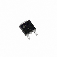
NDD03N60ZT4G ON Semiconductor, NDD03N60ZT4G Datasheet - Page 5

NDD03N60ZT4G
Manufacturer Part Number
NDD03N60ZT4G
Description
MOSFET N-CH 600V DPAK
Manufacturer
ON Semiconductor
Datasheet
1.NDF03N60ZG.pdf
(10 pages)
Specifications of NDD03N60ZT4G
Package / Case
DPak, DPak-3, SOT-223, TO-220, TO-220AB, TO-225AA, TO-92
Mounting Type
Surface Mount
Power - Max
61W
Fet Type
MOSFET N-Channel, Metal Oxide
Gate Charge (qg) @ Vgs
12nC @ 10V
Vgs(th) (max) @ Id
4.5V @ 50µA
Current - Continuous Drain (id) @ 25° C
2.6A
Drain To Source Voltage (vdss)
600V
Fet Feature
Standard
Rds On (max) @ Id, Vgs
3.6 Ohm @ 1.2A, 10V
Configuration
Single
Transistor Polarity
N-Channel
Resistance Drain-source Rds (on)
3.3 Ohms
Forward Transconductance Gfs (max / Min)
2 S
Drain-source Breakdown Voltage
600 V
Gate-source Breakdown Voltage
30 V
Continuous Drain Current
2.6 A
Power Dissipation
61 W
Maximum Operating Temperature
+ 125 C
Mounting Style
SMD/SMT
Gate Charge Qg
12 nC
Minimum Operating Temperature
- 55 C
Package
3DPAK
Channel Mode
Enhancement
Channel Type
N
Typical Fall Time
10 ns
Typical Rise Time
8 ns
Typical Turn-off Delay Time
16 ns
Typical Turn-on Delay Time
9 ns
Maximum Continuous Drain Current
2.6 A
Maximum Drain Source Voltage
600 V
Maximum Gate Source Voltage
30 V
Lead Free Status / RoHS Status
Lead free / RoHS Compliant
Available stocks
Company
Part Number
Manufacturer
Quantity
Price
Company:
Part Number:
NDD03N60ZT4G
Manufacturer:
ON
Quantity:
2 500
Company:
Part Number:
NDD03N60ZT4G
Manufacturer:
ON Semiconductor
Quantity:
336
Company:
Part Number:
NDD03N60ZT4G
Manufacturer:
ON
Quantity:
12 500
0.01
100
0.1
0.01
0.01
10
100
0.1
0.1
1
10
1E−06
10
1E−06
0.1
1
1
V
SINGLE PULSE
T
50% (DUTY CYCLE)
2.0%
1.0%
Figure 12. Maximum Rated Forward Biased
1.0%
5.0%
50% (DUTY CYCLE)
20%
10%
2.0%
5.0%
C
GS
20%
10%
= 25°C
v 30 V
SINGLE PULSE
V
SINGLE PULSE
Safe Operating Area NDD03N60Z
DS
, DRAIN−TO−SOURCE VOLTAGE (V)
1E−05
1E−05
1
Figure 15. Thermal Impedance (Junction−to−Ambient) for NDD03N60Z
Figure 14. Thermal Impedance (Junction−to−Case) for NDD03N60Z
1E−04
1E−04
10 ms
10
R
THERMAL LIMIT
PACKAGE LIMIT
DS(on)
1 ms
100 ms
dc
LIMIT
1E−03
1E−03
TYPICAL CHARACTERISTICS
100
10 ms
http://onsemi.com
1E−02
1E−02
PULSE TIME (s)
PULSE TIME (s)
1000
5
0.01
100
0.1
10
1
1E−01
1E−01
0.1
V
SINGLE PULSE
T
Figure 13. Maximum Rated Forward Biased
C
GS
= 25°C
v 30 V
V
Safe Operating Area NDF03N60Z
DS
, DRAIN−TO−SOURCE VOLTAGE (V)
1E+00
1E+00
1
1E+01
dc
1E+01
10 ms
10
R
THERMAL LIMIT
PACKAGE LIMIT
DS(on)
1 ms
LIMIT
R
Steady State
100 ms
R
Steady State
qJA
1E+02
1E+02
qJA
100
= 40°C/W
= 2°C/W
10 ms
1E+03
1E+03
1000


