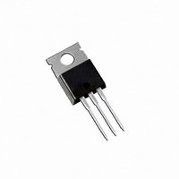
IRL3715 International Rectifier, IRL3715 Datasheet

IRL3715
Specifications of IRL3715
Available stocks
Related parts for IRL3715
IRL3715 Summary of contents
Page 1
... IRL3715 @ 10V GS @ 10V 94194A IRL3715 IRL3715S IRL3715L ® HEXFET Power MOSFET R max I DS(on) D 14m 54A 2 D Pak TO-262 IRL3715S IRL3715L Max. Units 20 ± 210 71 W 3.8 W 0.48 W/°C - 175 °C Typ. Max. Units ––– 2.1 0.50 ––– ...
Page 2
... IRL3715/S/L Static @ T = 25°C (unless otherwise specified) J Parameter V Drain-to-Source Breakdown Voltage (BR)DSS Breakdown Voltage Temp. Coefficient (BR)DSS J R Static Drain-to-Source On-Resistance DS(on) V Gate Threshold Voltage GS(th) I Drain-to-Source Leakage Current DSS Gate-to-Source Forward Leakage I GSS Gate-to-Source Reverse Leakage Dynamic @ T = 25°C (unless otherwise specified) ...
Page 3
... Fig 2. Typical Output Characteristics 2 2.0 1.5 ° J 1.0 0.5 = 15V 0.0 7.0 8.0 -60 -40 -20 0 Fig 4. Normalized On-Resistance IRL3715/S/L VGS 15V 10V 4.5V 3.5V 3.3V 3.0V 2.7V 2.5V 2.5V 20µs PULSE WIDTH ° 175 Drain-to-Source Voltage (V) DS 52A ...
Page 4
... IRL3715/S/L 10000 0V, C iss = rss = oss = Ciss 1000 Coss Crss 100 Drain-to-Source Voltage (V) Fig 5. Typical Capacitance Vs. Drain-to-Source Voltage 100 ° 175 0.1 0.2 0.7 1.2 V ,Source-to-Drain Voltage (V) SD Fig 7. Typical Source-Drain Diode Forward Voltage MHZ SHORTED 100 0 Fig 6. Typical Gate Charge Vs. ...
Page 5
... Fig 11. Maximum Effective Transient Thermal Impedance, Junction-to-Case www.irf.com R G 4.5V Pulse Width Duty Factor Fig 10a. Switching Time Test Circuit V DS 90% 150 175 ° 10 d(on) Fig 10b. Switching Time Waveforms Notes: 1. Duty factor Peak 0.001 t , Rectangular Pulse Duration (sec) 1 IRL3715/S D.U. µ d(off ...
Page 6
... IRL3715/S Fig 12a. Unclamped Inductive Test Circuit Fig 12b. Unclamped Inductive Waveforms Charge Fig 13a. Basic Gate Charge Waveform 6 240 1 5V 200 160 + - 120 Starting T , Junction Temperature ( C) Fig 12c. Maximum Avalanche Energy Fig 13b. Gate Charge Test Circuit I D TOP 8 ...
Page 7
... Ground Plane Low Leakage Inductance Current Transformer - - + dv/dt controlled Driver same type as D.U.T. I controlled by Duty Factor "D" SD D.U.T. - Device Under Test P.W. Period D = Period Body Diode Forward Current di/dt Diode Recovery dv/dt Body Diode Forward Drop Ripple 5% ® Power MOSFETs IRL3715/S =10V ...
Page 8
... IRL3715/S/L TO-220AB Package Outline Dimensions are shown in millimeters (inches (. (. (. (. (. (. (. (. (. (. (. & TO-220AB Part Marking Information (. (. (. (. 6 6 & (. (. (. (. (. (. www.irf.com ...
Page 9
... D Pak Package Outline 2 D Pak Part Marking Information www.irf.com IRL3715/S/L 9 ...
Page 10
... IRL3715/S/L TO-262 Package Outline TO-262 Part Marking Information 10 www.irf.com ...
Page 11
... This is only applied to TO-220A package Data and specifications subject to change without notice. This product has been designed and qualified for the Industrial market. Qualification Standards can be found on IR’s Web site. Visit us at www.irf.com for sales contact information. 6/01 IRL3715/S .42 (. ...
Page 12
Note: For the most current drawings please refer to the IR website at: http://www.irf.com/package/ ...


