IRF2804S-7P International Rectifier, IRF2804S-7P Datasheet
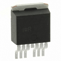
MOSFET N-CH 40V 160A D2PAK7

IRF2804S-7P

Manufacturer Part Number
IRF2804S-7P
Description
MOSFET N-CH 40V 160A D2PAK7
Manufacturer
International Rectifier
Series
HEXFET®r
Datasheet

Specifications of IRF2804S-7P

Fet Type
MOSFET N-Channel, Metal Oxide
Fet Feature
Standard
Rds On (max) @ Id, Vgs
1.6 mOhm @ 160A, 10V
Drain To Source Voltage (vdss)
40V
Current - Continuous Drain (id) @ 25° C
160A
Vgs(th) (max) @ Id
4V @ 250µA
Gate Charge (qg) @ Vgs
260nC @ 10V
Input Capacitance (ciss) @ Vds
6930pF @ 25V
Power - Max
330W
Mounting Type
Surface Mount
Package / Case
D²Pak, TO-263 (6 leads + tab)
Lead Free Status / RoHS Status
Contains lead / RoHS non-compliant
Other names
*IRF2804S-7P

Available stocks

Company
Part Number
Manufacturer
Quantity
Price
Part Number:
IRF2804S-7P
Manufacturer:
IR/INFINEON
Quantity:
20 000
Features
l
l
l
l
l
Description
Specifically designed for Automotive applications,
this HEXFET
processing techniques to achieve extremely low
on-resistance per silicon area. Additional fea-
tures of this design are a 175°C junction operat-
ing temperature, fast switching speed and im-
proved repetitive avalanche rating . These fea-
tures combine to make this design an extremely
efficient and reliable device for use in Automotive
applications and a wide variety of other applica-
tions.
HEXFET
Absolute Maximum Ratings
I
I
I
I
P
V
E
E
I
E
T
T
Thermal Resistance
R
R
R
R
www.irf.com
D
D
D
DM
AR
J
STG
D
GS
AS
AS
AR
θJC
θCS
θJA
θJA
@ T
@ T
@ T
Advanced Process Technology
Ultra Low On-Resistance
175°C Operating Temperature
Fast Switching
Repetitive Avalanche Allowed up to Tjmax
@T
(tested)
C
C
C
C
= 25°C
= 100°C
= 25°C
= 25°C
®
is a registered trademark of International Rectifier.
®
Power MOSFET utilizes the latest
Continuous Drain Current, V
Pulsed Drain Current
Maximum Power Dissipation
Linear Derating Factor
Gate-to-Source Voltage
Single Pulse Avalanche Energy (Thermally Limited)
Single Pulse Avalanche Energy Tested Value
Avalanche Current
Repetitive Avalanche Energy
Operating Junction and
Storage Temperature Range
Soldering Temperature, for 10 seconds
Mounting torque, 6-32 or M3 screw
Junction-to-Case
Case-to-Sink, Flat, Greased Surface
Junction-to-Ambient
Junction-to-Ambient (PCB Mount, steady state)
j
j
Parameter
Parameter
AUTOMOTIVE MOSFET
GS
GS
GS
g
@ 10V (Silicon Limited)
@ 10V (See Fig. 9)
@ 10V
(Package Limited)
h
G
ij
d
300 (1.6mm from case )
HEXFET
See Fig.12a,12b,15,16
IRF2804S-7P
Typ.
S
0.50
D
–––
–––
–––
10 lbf•in (1.1N•m)
-55 to + 175
Max.
1360
1050
320
230
160
330
± 20
630
2.2
®
R
Power MOSFET
DS(on)
Max.
0.50
V
–––
62
40
I
DSS
D
= 160A
PD - 96891A
= 1.6mΩ
= 40V
D
Units
Units
W/°C
°C/W
mJ
mJ
°C
W
A
V
A
1

Related parts for IRF2804S-7P

IRF2804S-7P Summary of contents

Page 1

... HEXFET is a registered trademark of International Rectifier. www.irf.com AUTOMOTIVE MOSFET G Parameter @ 10V (Silicon Limited 10V (See Fig 10V (Package Limited Parameter 96891A IRF2804S-7P ® HEXFET Power MOSFET 40V DSS R = 1.6mΩ DS(on 160A D D Max. Units 320 A 230 160 1360 ...

Page 2

Static @ T = 25°C (unless otherwise specified) J Parameter V Drain-to-Source Breakdown Voltage (BR)DSS ∆ΒV /∆T Breakdown Voltage Temp. Coefficient DSS J R SMD Static Drain-to-Source On-Resistance DS(on) V Gate Threshold Voltage GS(th) gfs Forward Transconductance I Drain-to-Source Leakage ...

Page 3

PULSE WIDTH 4. 25° Drain-to-Source Voltage (V) Fig 1. Typical Output Characteristics 1000.0 100 175°C 10 25°C 1 ...

Page 4

0V MHZ C iss = SHORTED 12000 C rss = oss = 10000 8000 Ciss 6000 4000 ...

Page 5

LIMITED BY PACKAGE 300 250 200 150 100 100 Case Temperature (°C) Fig 9. Maximum Drain Current vs. Case Temperature 0.50 0.1 0.20 0.10 0.05 0.01 0.02 0.01 ...

Page 6

D.U 20V GS 0.01 Ω Fig 12a. Unclamped Inductive Test Circuit V (BR)DSS Fig 12b. Unclamped Inductive Waveforms ...

Page 7

Duty Cycle = Single Pulse 1000 0.01 100 0.05 0. 0.1 1.0E-06 1.0E-05 Fig 15. Typical Avalanche Current vs.Pulsewidth 800 TOP Single Pulse BOTTOM 1% Duty Cycle 160A 600 400 200 ...

Page 8

D.U.T + ƒ • • - • + ‚ -  • • • SD • Fig 17. Fig 18a. Switching Time Test Circuit V DS 90% 10 Fig 18b. Switching Time Waveforms 8 Driver Gate Drive P.W. ...

Page 9

D Pak - 7 Pin Package Outline Dimensions are shown in millimeters (inches Pak - 7 Pin Part Marking Information www.irf.com 25 9 ...

Page 10

D Pak - 7 Pin Tape and Reel This product has been designed and qualified for the Automotive [Q101]market. IR WORLD HEADQUARTERS: 233 Kansas St., El Segundo, California 90245, USA Tel: (310) 252-7105 10 Data and specifications subject to ...

Page 11

Note: For the most current drawings please refer to the IR website at: http://www.irf.com/package/ ...

Related keywords