NTY100N10G ON Semiconductor, NTY100N10G Datasheet - Page 3
NTY100N10G
Manufacturer Part Number
NTY100N10G
Description
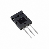
MOSFET N-CH 100V 123A TO-264
Manufacturer
ON Semiconductor
Datasheet
1.NTY100N10.pdf
(8 pages)
Specifications of NTY100N10G
Fet Type
MOSFET N-Channel, Metal Oxide
Fet Feature
Standard
Rds On (max) @ Id, Vgs
10 mOhm @ 50A, 10V
Drain To Source Voltage (vdss)
100V
Current - Continuous Drain (id) @ 25° C
123A
Vgs(th) (max) @ Id
4V @ 250µA
Gate Charge (qg) @ Vgs
350nC @ 10V
Input Capacitance (ciss) @ Vds
10110pF @ 25V
Power - Max
313W
Mounting Type
Through Hole
Package / Case
TO-264-3, TO-3BPL
Lead Free Status / RoHS Status
Lead free / RoHS Compliant
Available stocks
Company
Part Number
Manufacturer
Quantity
Price
Company:

Part Number:
NTY100N10G
Manufacturer:
OMNLREL
Quantity:
12 500


0.018
0.016
0.014
0.012
0.008
0.006
0.004
0.002
0.01
200
150
100
2.5
2.0
1.5
1.0
0.5
50
0
0
0
−50
0
0
V
I
V
D
GS
GS
= 50 A
−25
Figure 5. On−Resistance Variation with
Figure 3. On−Resistance versus Drain
= 10 V
= 10 V
Figure 1. On−Region Characteristics
V
DS
2
T
J
, DRAIN−TO−SOURCE VOLTAGE (V)
, JUNCTION TEMPERATURE (°C)
0
50
Current and Temperature
V
I
GS
D
V
V
, DRAIN CURRENT (A)
V
GS
= 6.5 V
GS
GS
25
Temperature
4
= 8.0 V
= 7.0 V
= 9.0 V
T = 100°C
T = −55°C
T = 25°C
50
100
V
6
GS
75
= 10 V
V
V
V
V
GS
GS
GS
GS
100
150
T
= 6.0 V
= 5.6 V
= 5.0 V
= 4.6 V
J
8
= 25°C
http://onsemi.com
125
200
150
10
3
1000000
100000
0.0095
0.0085
0.0075
10000
0.009
0.008
1000
200
150
100
100
1.0
50
10
0
0
0
0
T = 25°C
V
V
DS
GS
w 10 V
Figure 2. On−Region Characteristics
= 0 V
V
V
Figure 4. On−Resistance versus Drain
DS
V
GS
Figure 6. Drain−to−Source Leakage
20
2
GS
, DRAIN−TO−SOURCE VOLTAGE (V)
T
, GATE−TO−SOURCE VOLTAGE (V)
50
J
= 10 V
V
= 100°C
T
T
Current and Gate Voltage
GS
J
J
Current versus Voltage
= 100°C
I
= 125°C
D
= 15 V
, DRAIN CURRENT (A)
40
4
100
T
60
6
J
T
= 25°C
J
= −55°C
150
80
8
10
100
20
Related parts for NTY100N10G
Image
Part Number
Description
Manufacturer
Datasheet
Request
R

Part Number:
Description:
ON Semiconductor [VOLTAGE REGULATOR]
Manufacturer:
ON Semiconductor
Datasheet:
Part Number:
Description:
357-036-542-201 CARDEDGE 36POS DL .156 BLK LOPRO
Manufacturer:
ON Semiconductor
Datasheet:
Part Number:
Description:
357-036-542-201 CARDEDGE 36POS DL .156 BLK LOPRO
Manufacturer:
ON Semiconductor
Datasheet:
Part Number:
Description:
357-036-542-201 CARDEDGE 36POS DL .156 BLK LOPRO
Manufacturer:
ON Semiconductor
Datasheet:
Part Number:
Description:
357-036-542-201 CARDEDGE 36POS DL .156 BLK LOPRO
Manufacturer:
ON Semiconductor
Datasheet:
Part Number:
Description:
357-036-542-201 CARDEDGE 36POS DL .156 BLK LOPRO
Manufacturer:
ON Semiconductor
Datasheet:
Part Number:
Description:
357-036-542-201 CARDEDGE 36POS DL .156 BLK LOPRO
Manufacturer:
ON Semiconductor
Datasheet:
Part Number:
Description:
357-036-542-201 CARDEDGE 36POS DL .156 BLK LOPRO
Manufacturer:
ON Semiconductor
Datasheet:
Part Number:
Description:
357-036-542-201 CARDEDGE 36POS DL .156 BLK LOPRO
Manufacturer:
ON Semiconductor
Datasheet:
Part Number:
Description:
357-036-542-201 CARDEDGE 36POS DL .156 BLK LOPRO
Manufacturer:
ON Semiconductor
Datasheet:
Part Number:
Description:
357-036-542-201 CARDEDGE 36POS DL .156 BLK LOPRO
Manufacturer:
ON Semiconductor
Datasheet:
Part Number:
Description:
Manufacturer:
ON Semiconductor
Datasheet:
Part Number:
Description:
Manufacturer:
ON Semiconductor
Datasheet:
Part Number:
Description:
Manufacturer:
ON Semiconductor
Datasheet: