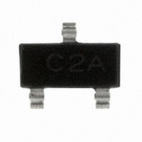
HSMS-2822-TR1G Avago Technologies US Inc., HSMS-2822-TR1G Datasheet - Page 4

HSMS-2822-TR1G
Manufacturer Part Number
HSMS-2822-TR1G
Description
DIODE SCHOTTKY RF SER 15V SOT-23
Manufacturer
Avago Technologies US Inc.
Datasheet
1.HSMS-2823-BLKG.pdf
(15 pages)
Specifications of HSMS-2822-TR1G
Package / Case
SOT-23-3, TO-236-3, Micro3™, SSD3, SST3
Diode Type
Schottky - 1 Pair Series Connection
Voltage - Peak Reverse (max)
15V
Current - Max
1A
Capacitance @ Vr, F
1pF @ 0V, 1MHz
Resistance @ If, F
12 Ohm @ 5mA, 1MHz
Product
Schottky Diodes
Peak Reverse Voltage
15 V
Forward Continuous Current
1 A
Configuration
Dual Series
Forward Voltage Drop
0.5 V @ 0.01 A
Maximum Reverse Leakage Current
0.1 uA @ 1 V
Operating Temperature Range
+ 150 C
Mounting Style
SMD/SMT
Capacitance Ct
1pF
Diode Case Style
SOT-23
No. Of Pins
3
Breakdown Voltage
15V
Forward Voltage
340mV
Leaded Process Compatible
Yes
Rohs Compliant
Yes
Forward Current If Max
1A
Forward Voltage Vf Max
340mV
Lead Free Status / RoHS Status
Lead free / RoHS Compliant
Power Dissipation (max)
-
Lead Free Status / Rohs Status
Lead free / RoHS Compliant
Other names
516-1818-2
HSMS-2822-TR1G
HSMS-2822-TR1G
Available stocks
Company
Part Number
Manufacturer
Quantity
Price
Company:
Part Number:
HSMS-2822-TR1G
Manufacturer:
AVAGO
Quantity:
5 667
Company:
Part Number:
HSMS-2822-TR1G
Manufacturer:
AVAGO
Quantity:
2 000
Part Number:
HSMS-2822-TR1G
Manufacturer:
AVAGO/安华高
Quantity:
20 000
4
Typical Performance, T
Figure 1. Forward Current vs. Forward Voltage at
Temperatures.
Figure 4. Dynamic Resistance vs. Forward
Current.
Figure 7. Typical Output Voltage vs. Input Power,
Small Signal Detector Operating at 850 MHz.
0.001
1000
0.01
0.01
100
100
0.1
0.1
10
10
1
1
1
0.1
-40
0
T
T
T
T
DC bias = 3 A
A
A
A
A
= +125C
= +75C
= +25C
= –25C
0.10
I
F
V
F
– FORWARD CURRENT (mA)
-30
P
in
– FORWARD VOLTAGE (V)
RF in
– INPUT POWER (dBm)
1
0.20
3.3 nH
18 nH
-20
0.30
100 pF
C
HSMS-282B
10
= 25°C (unless otherwise noted), Single Diode
-10
0.40
100 K
-25C
+25C
+75C
Vo
0.50
100
0
100,000
Figure 2. Reverse Current vs. Reverse Voltage at
Temperatures.
Figure 8. Typical Output Voltage vs. Input Power,
Large Signal Detector Operating at 915 MHz.
1E-005
10,000
Figure 5. Typical V
at Mixer Bias Levels.
0.0001
0.001
1000
0.01
100
0.3
0.1
30
10
10
10
1
1
1
-20
0.2
0
+25C
0.4
-10
V
V
F
P
R
in
- FORWARD VOLTAGE (V)
– REVERSE VOLTAGE (V)
RF in
– INPUT POWER (dBm)
f
68
0.6
5
Match, Series Pairs and Quads
0
0.8
I
T
T
T
F
HSMS-282B
V
A
A
A
(Left Scale)
10
F
= +125C
= +75C
= +25C
100 pF
(Right Scale)
10
1.0
20
1.2
4.7 K
Vo
15
1.4
30
30
10
1
0.3
Figure 3. Total Capacitance vs. Reverse Voltage.
Figure 9. Typical Conversion Loss vs. L.O. Drive,
2.0 GHz (Ref AN997).
Figure 6. Typical V
Bias Levels.
100
0.8
0.6
0.4
0.2
10
10
1
9
8
7
6
1
0
0.10
0
LOCAL OSCILLATOR POWER (dBm)
0
V
V
F
R
2
- FORWARD VOLTAGE (V)
– REVERSE VOLTAGE (V)
2
0.15
f
Match, Series Pairs at Detector
4
4
V
F
6
(Right Scale)
I
0.20
F
(Left Scale)
8
6
10
0.25
12
8
1.0
0.1


