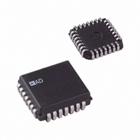
DAC8412FPC Analog Devices Inc, DAC8412FPC Datasheet - Page 8

DAC8412FPC
Manufacturer Part Number
DAC8412FPC
Description
DAC 4-CH R-2R 12-Bit 28-Pin PLCC
Manufacturer
Analog Devices Inc
Datasheet
1.DAC8412FPCZ.pdf
(20 pages)
Specifications of DAC8412FPC
Package
28PLCC
Resolution
12 Bit
Conversion Rate
167 KSPS
Architecture
R-2R
Digital Interface Type
Parallel
Number Of Outputs Per Chip
4
Output Type
Voltage
Full Scale Error
±8 LSB
Integral Nonlinearity Error
±4 LSB
Maximum Settling Time
10(Typ) us
Rohs Status
RoHS non-compliant
Settling Time
6µs
Number Of Bits
12
Data Interface
Parallel
Number Of Converters
4
Voltage Supply Source
Single Supply
Power Dissipation (max)
330mW
Operating Temperature
-40°C ~ 85°C
Mounting Type
Surface Mount
Package / Case
28-LCC (J-Lead)
Number Of Channels
4
Interface Type
Parallel
Single Supply Voltage (typ)
5V
Dual Supply Voltage (typ)
±15V
Power Supply Requirement
Single/Dual
Single Supply Voltage (min)
4.75V
Single Supply Voltage (max)
5.25V
Dual Supply Voltage (min)
±14.25V
Dual Supply Voltage (max)
±15.75V
Operating Temp Range
-40C to 85C
Operating Temperature Classification
Industrial
Mounting
Surface Mount
Pin Count
28
Package Type
PLCC
Lead Free Status / Rohs Status
Not Compliant
Available stocks
Company
Part Number
Manufacturer
Quantity
Price
Company:
Part Number:
DAC8412FPC
Manufacturer:
AD
Quantity:
1 000
Company:
Part Number:
DAC8412FPC
Manufacturer:
Analog Devices Inc
Quantity:
10 000
Part Number:
DAC8412FPC
Manufacturer:
ADI/亚德诺
Quantity:
20 000
Company:
Part Number:
DAC8412FPC-REEL
Manufacturer:
Analog Devices Inc
Quantity:
10 000
Company:
Part Number:
DAC8412FPCZ
Manufacturer:
TI
Quantity:
650
Company:
Part Number:
DAC8412FPCZ
Manufacturer:
ADI33
Quantity:
176
Company:
Part Number:
DAC8412FPCZ
Manufacturer:
Analog Devices Inc
Quantity:
10 000
Part Number:
DAC8412FPCZ
Manufacturer:
ADI/亚德诺
Quantity:
20 000
Company:
Part Number:
DAC8412FPCZ-REEL
Manufacturer:
Analog Devices Inc
Quantity:
10 000
DAC8412/DAC8413
PIN CONFIGURATION AND FUNCTION DESCRIPTIONS
DB0 (LSB)
Table 5. Pin Function Descriptions
Pin Number
1
2
3
4
5
6
7
8
9
10
11
12
13
14
15
16
17
18
19
20
21
22
23
24
25
26
27
28
RESET
V
V
V
DGND
LDAC
OUTB
OUTA
REFH
DB1
DB2
DB3
DB4
DB5
DB6
V
SS
10
11
12
13
14
Figure 7. PDIP/CERDIP
1
2
3
4
5
6
7
8
9
(Not to Scale)
DAC8412/
DAC8413
TOP VIEW
Mnemonic
V
V
V
V
DGND
RESET
LDAC
DB0
DB1
DB2
DB3
DB4
DB5
DB6
DB7
DB8
DB9
DB10
DB11
R/W
A1
A0
CS
V
V
V
V
V
REFH
OUTB
OUTA
SS
LOGIC
DD
OUTD
OUTC
REFL
28
27
26
25
24
23
22
21
20
19
18
17
16
15
V
V
V
V
V
CS
A0
A1
R/W
DB11 (MSB)
DB10
DB9
DB8
DB7
REFL
OUTC
OUTD
DD
LOGIC
Description
High-Side DAC Reference Input.
DAC B Output.
DAC A Output.
Lower Rail Power Supply.
Digital Ground.
Reset Input and Output Registers to all 0s, Enabled at Active Low.
Load Data to DAC, Enabled at Active Low.
Data Bit 0, LSB.
Data Bit 1.
Data Bit 2.
Data Bit 3.
Data Bit 4.
Data Bit 5.
Data Bit 6.
Data Bit 7.
Data Bit 8.
Data Bit 9.
Data Bit 10.
Data Bit 11, MSB.
Active Low to Write Data to DAC. Active high to readback previous data at data bit pins with V
Address Bit 1.
Address Bit 0.
Chip Select, Enabled at Active Low.
Voltage Supply for Readback Function. Can be open circuit if not used.
Upper Rail Power Supply.
DAC D Output.
DAC C Output.
Low-Side DAC Reference Input.
DB0 (LSB)
RESET
DGND
LDAC
DB1
DB2
DB3
10
11
5
6
7
8
9
INDENTFIER
12
4
13 14
3
(Not to Scale)
DAC8412/
DAC8413
Figure 8. PLCC
TOP VIEW
PIN 1
2
Rev. F | Page 8 of 20
15
1
16 17
28
27 26
18
25
24
23
22
21
20
19
V
V
CS
A0
A1
R/W
DB11 (MSB)
DD
LOGIC
DB0 (LSB)
RESET
DGND
LDAC
DB1
DB2
DB3
10
11
5
6
7
8
9
12
4
13
3
DAC8412/
(Not to Scale)
DAC8413
TOP VIEW
Figure 9. LCC
14
2
15
1
28
16
27
17
LOGIC
26
18
connected to 5 V.
25
24
23
22
21
20
19
V
V
CS
A0
A1
R/W
DB11 (MSB)
DD
LOGIC


