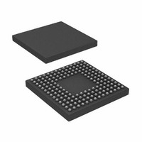
ADSP-BF533SBBC500 Analog Devices Inc, ADSP-BF533SBBC500 Datasheet - Page 13

ADSP-BF533SBBC500
Manufacturer Part Number
ADSP-BF533SBBC500
Description
DSP Fixed-Point 16-Bit 500MHz 500MIPS 160-Pin CSP-BGA
Manufacturer
Analog Devices Inc
Series
Blackfin®r
Type
Fixed Pointr
Datasheet
1.ADSP-BF531SBSTZ400.pdf
(12 pages)
Specifications of ADSP-BF533SBBC500
Package
160CSP-BGA
Numeric And Arithmetic Format
Fixed-Point
Maximum Speed
500 MHz
Device Million Instructions Per Second
500 MIPS
Rohs Status
RoHS non-compliant
Interface
SPI, SSP, UART
Clock Rate
500MHz
Non-volatile Memory
ROM (1 kB)
On-chip Ram
148kB
Voltage - I/o
1.8V, 2.5V, 3.3V
Voltage - Core
1.20V
Operating Temperature
-40°C ~ 85°C
Mounting Type
Surface Mount
Package / Case
160-CSPBGA
For Use With
ADZS-BFAUDIO-EZEXT - BOARD EVAL AUDIO BLACKFINADZS-BFAV-EZEXT - BOARD DAUGHT ADSP-BF533,37,61KITADZS-BF533-EZLITE - KIT W/BOARD EVAL FOR ADSP-BF533
Lead Free Status / RoHS Status
Available stocks
Company
Part Number
Manufacturer
Quantity
Price
Company:
Part Number:
ADSP-BF533SBBC500
Manufacturer:
ADI
Quantity:
210
Company:
Part Number:
ADSP-BF533SBBC500
Manufacturer:
Analog Devices Inc
Quantity:
10 000
Silicon Anomaly List
20.
21.
22.
DESCRIPTION:
The problem can occur when 3 or more consecutive DMA reads from a single L1 memory bank (Bank A or Bank B) are stalled for an
extended period of time (due to core or cache activity). In this situation, when a subsequent L1 DMA read is initiated from a different
bank, it is possible that the data from the last 2 reads will collide, corrupting the data.
WORKAROUND:
There are two workarounds for this issue:
1) Locate all DMA data within the same L1 memory bank (for example, bank A or bank B).
2) Ensure that only 1 DMA Channel reads from a given L1 memory bank at any given time.
APPLIES TO REVISION(S):
0.3
DESCRIPTION:
When Writethrough cache is enabled and DCPLB_DATAx:CPLB_L1_AOW = 0 (Allocate Cache Lines on Reads Only), incorrect data may be
read in the following scenario:
• Must write to an address which is writethrough cacheable in no-allocate-on-write mode, and cache miss must occur
• Must read above address while write is still in Store buffer (not yet in Write buffer or destination memory location)
• Must then read above address again after it drains from Store buffer. Data returned from cache will be incorrect but the destination
memory location will have correct value.
WORKAROUND:
When configuring data cache as writethrough, set DCPLB_DATAx:CPLB_L1_AOW = 1 (allocate cache lines on reads and writes) to avoid
the possibility of this anomaly.
APPLIES TO REVISION(S):
0.3
DESCRIPTION:
When a "brown-out" occurs, the internal Voltage regulator cannot be reset using the hardware reset pin. A "brown-out" is defined as a
condition in which VDDext drops below the range specified in the data sheet, but does not drop all the way to 0 V, before it returns to the
proper value.
WORKAROUND:
In order to recover from a "brown-out", the processor must be powered down completely and then powered back up.
APPLIES TO REVISION(S):
0.3
05000203 - Specific Sequence That Can Cause DMA Error or DMA Stopping:
05000204 - Incorrect Data Read with Writethrough "Allocate Cache Lines on Reads Only" Cache Mode:
05000207 - Recovery from "Brown-Out" Condition:
NR003532D | Page 13 of 45 | July 2008
ADSP-BF531/BF532/BF533


