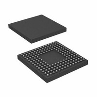
ADSP-BF533SBBC500 Analog Devices Inc, ADSP-BF533SBBC500 Datasheet - Page 44

ADSP-BF533SBBC500
Manufacturer Part Number
ADSP-BF533SBBC500
Description
DSP Fixed-Point 16-Bit 500MHz 500MIPS 160-Pin CSP-BGA
Manufacturer
Analog Devices Inc
Series
Blackfin®r
Type
Fixed Pointr
Datasheet
1.ADSP-BF531SBSTZ400.pdf
(12 pages)
Specifications of ADSP-BF533SBBC500
Package
160CSP-BGA
Numeric And Arithmetic Format
Fixed-Point
Maximum Speed
500 MHz
Device Million Instructions Per Second
500 MIPS
Rohs Status
RoHS non-compliant
Interface
SPI, SSP, UART
Clock Rate
500MHz
Non-volatile Memory
ROM (1 kB)
On-chip Ram
148kB
Voltage - I/o
1.8V, 2.5V, 3.3V
Voltage - Core
1.20V
Operating Temperature
-40°C ~ 85°C
Mounting Type
Surface Mount
Package / Case
160-CSPBGA
For Use With
ADZS-BFAUDIO-EZEXT - BOARD EVAL AUDIO BLACKFINADZS-BFAV-EZEXT - BOARD DAUGHT ADSP-BF533,37,61KITADZS-BF533-EZLITE - KIT W/BOARD EVAL FOR ADSP-BF533
Lead Free Status / RoHS Status
Available stocks
Company
Part Number
Manufacturer
Quantity
Price
Company:
Part Number:
ADSP-BF533SBBC500
Manufacturer:
ADI
Quantity:
210
Company:
Part Number:
ADSP-BF533SBBC500
Manufacturer:
Analog Devices Inc
Quantity:
10 000
ADSP-BF531/BF532/BF533
76.
77.
78.
DESCRIPTION:
When the PPI port is configured in transmit mode with two internal frame syncs, the PPI will not start properly if the PPI Frame Sync 3
(PPI_FS3) pin is left floating.
WORKAROUND:
The PPI_FS3 pin must be pulled down when the PPI is configured in transmit mode with 2 internal frame syncs.
APPLIES TO REVISION(S):
0.5
DESCRIPTION:
Executing an SSYNC instruction from non-cacheable L2 memory with interrupts disabled can cause the processor to stall.
WORKAROUND:
If any interrupts are enabled, the stall will still occur, but it will be broken by the asynchronous event. If no interrupts are enabled or no
interrupts are being generated, the stall is indefinite and the processor must be reset.
To avoid the stall condition, the following conditions must be met.
1) The SSYNC is in L1 memory or in cacheable L2 memory.
2) The SSYNC is not at a loop bottom where the loop top is located in non-cacheable L2 memory.
3) If the SSYNC is located in a cacheable L2 page, it is at least eight 64-bit words away from the bottom of the page (as specified by a
CPLB) if the following (address sequential) page is either L1 or non-cacheable L2 memory.
If any of the above conditions is not met, another workaround would be to configure one of the timers prior to the SSYNC instruction with
a time-out period to generate an interrupt and break the stall.
APPLIES TO REVISION(S):
0.5
DESCRIPTION:
When level-sensitive GPIO events are used to wake the processor from the low-power sleep mode of operation, the processor may stall
indefinitely if the width of the wakeup pulse is too short. When this occurs, the PLL begins transitioning from the sleep mode due to the
level sensed on the GPIO pin, but then reverts back to the sleep mode if the trigger level is removed before the core has had sufficient
time to break the idle state to resume execution.
As a result, the processor does not wake up properly, at which point only a hardware reset can exit the resulting stall condition.
WORKAROUND:
There are two ways to avoid this anomaly:
1) Use edge-sensitivity for the pin(s) being used to generate the wakeup event.
2) Ensure that the edge on the wakeup signal is clean and held at the trigger level for at least 3 system clock (SCLK) cycles.
APPLIES TO REVISION(S):
0.3, 0.4, 0.5, 0.6
05000400 - PPI Does Not Start Properly In Specific Mode:
05000402 - SSYNC Stalls Processor when Executed from Non-Cacheable Memory:
05000403 - Level-Sensitive External GPIO Wakeups May Cause Indefinite Stall:
NR003532D | Page 44 of 45 | July 2008
Silicon Anomaly List


