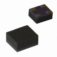
HMPP-3892-TR1 Avago Technologies US Inc., HMPP-3892-TR1 Datasheet

HMPP-3892-TR1
Specifications of HMPP-3892-TR1
Available stocks
Related parts for HMPP-3892-TR1
HMPP-3892-TR1 Summary of contents
Page 1
... Note that Avago’s manufacturing techniques assure that dice packaged in pairs are taken from adjacent sites on the wafer, assuring the highest degree of match. The HMPP-389T low inductance wide band shunt switch is well suited for applications GHz. Minipak 1412 is a ceramic based package, while Minipak QFN is a leadframe based package ...
Page 2
... HMPP-389x Series Absolute Maximum Ratings Symbol Parameter I Forward Current (1 µs pulse Peak Inverse Voltage IV T Junction Temperature j T Storage Temperature stg q Thermal Resistance [2] jc Notes: 1. Operation in excess of any one of these conditions may result in permanent damage to the device +25°C, where T is defined to be the temperature at the package pins where contact is ...
Page 3
... MiniPak 1412 HMPP-389x Series Typical Performance = +25 °C (unless otherwise noted), each diode 0 100 I – FORWARD BIAS CURRENT (mA) F Figure 1. Total RF Resistance vs. Forward Bias Current. 200 160 V = –2V R 120 – –10V FORWARD CURRENT (mA) Figure 4. Typical Reverse Recovery Time vs. Reverse Voltage. 3 0.50 0.45 ...
Page 4
Typical Applications RF COMMON BIAS 1 BIAS 2 Figure 6. Simple SPDT Switch Using Only Positive Bias. RF COMMON BIAS Figure 8. Very High ...
Page 5
... Given a thin epitaxial I region, the diode designer can trade off the device’s total resistance (R capacitance (C and I region. The HMPP-3890 was designed with the 930 MHz cellular and RFID, the 1.8 GHz PCS and 2.45 GHz RFID markets in mind. Combining the low resistance shown in Figure 15 with a typical total capacitance of 0 ...
Page 6
... Linear Equivalent Circuit In order to predict the performance of the HMPP-3890 as a switch necessary to construct a model which can then be used in one of the several linear analysis programs presently on the market. Such a model is given in Figure 16, where given in Figure 1 and Figure 2. Careful examination of Figure 16 will reveal ...
Page 7
... Testing the HMPP-389T on the Demo-board Introduction The HMPP-389T PIN diode is a high frequency shunt switch. It has been designed as a smaller and higher performance version of the HSMP-389T (SC-70 package). The DEMO-HMPP-389T demo-board allows customers to evaluate the performance of the HMPP-389T without having to fabricate their own PCB. Since a shunt switch’s isolation is limited primarily by its parasitic inductance, the product’ ...
Page 8
... FREQUENCY (GHz) Figure 17. Return Loss of HMPP-389T Mounted on Test Line at 0V and -20V Bias. Figure 18. Return loss of HMPP-389T mounted on test line at 0V and -20V bias. Normalization was used to remove the pcb’s and connec- tors’ losses from the measurement of the shunt switch’s loss ...
Page 9
Assembly Information The MiniPak diode is mounted to the PCB or microstrip board using the pad pattern shown in Figure 26. 0.4 0.5 0.4 Figure 21. PCB Pad Layout, MiniPak (dimensions in mm). This mounting pad pattern is satisfactory for ...
Page 10
... MiniPak 1412 Outline Drawing for HMPP-3890, -3892, and -3895 1.44 (0.057) 1.40 (0.055) 1.20 (0.047) 1.16 (0.046) Top view 0.70 (0.028) 0.58 (0.023) Side view Dimensions are in millimeters (inches) MiniPak 1412 Outline Drawing for HMPP-389T 0.92 (0.036) 0.00 0.88 (0.035) -0.07 (-0.003) ...
Page 11
... Ordering Information Part Number No. of Devices HMPP-389x-TR2 10000 HMPP-389x-TR1 3000 HMPP-389x-BLK 100 Device Orientation REEL USER FEED DIRECTION COVER TAPE 11 Container 13” Reel 7”Reel antistatic bag CARRIER TAPE 8 mm Note: “AA” represents package marking code. Package marking is right side up with carrier tape perforations at top. Conforms to Electronic Industries RS-481, “ ...
Page 12
Tape Dimensions and Product Orientation For Outline 4T (MiniPak 1412 DESCRIPTION CAVITY LENGTH WIDTH DEPTH PITCH BOTTOM HOLE DIAMETER PERFORATION DIAMETER PITCH POSITION CARRIER TAPE WIDTH THICKNESS COVER TAPE WIDTH TAPE THICKNESS DISTANCE CAVITY TO PERFORATION ...


