ATF-58143-BLKG Avago Technologies US Inc., ATF-58143-BLKG Datasheet

IC PHEMT 2GHZ 3V 30MA SOT-343

ATF-58143-BLKG

Manufacturer Part Number
ATF-58143-BLKG
Description
IC PHEMT 2GHZ 3V 30MA SOT-343
Manufacturer
Avago Technologies US Inc.
Datasheet

Specifications of ATF-58143-BLKG

Package / Case
SC-70-4, SC-82-4, SOT-323-4, SOT-343
Transistor Type
pHEMT FET
Frequency
2GHz
Gain
16.5dB
Voltage - Rated
5V
Current Rating
100mA
Noise Figure
0.5dB
Current - Test
30mA
Voltage - Test
3V
Power - Output
19dBm
Configuration
Single Dual Source
Power Dissipation
500 mW
Drain Source Voltage Vds
5 V
Gate-source Breakdown Voltage
- 5 V to 1 V
Continuous Drain Current
100 mA
Maximum Operating Temperature
+ 150 C
Maximum Drain Gate Voltage
- 5 V to 1 V
Minimum Operating Temperature
- 65 C
Mounting Style
SMD/SMT
Gate-source Voltage (max)
1V
Pin Count
3 +Tab
Drain-gate Voltage (max)
-5 to 1V
Drain-source Volt (max)
5V
Operating Temperature (min)
-65C
Operating Temperature (max)
150C
Operating Temperature Classification
Military
Mounting
Surface Mount
Package Type
SOT-343
Continuous Drain Current Id
500mA
Power Dissipation Pd
500mW
Noise Figure Typ
0.5dB
Rf Transistor Case
SC-70
No. Of Pins
4
Drain Current Idss Max
30mA
Rohs Compliant
Yes
Lead Free Status / RoHS Status
Lead free / RoHS Compliant
Lead Free Status / RoHS Status
Lead free / RoHS Compliant, Lead free / RoHS Compliant
Other names
516-1870
ATF-58143-BLKG

Available stocks

Company
Part Number
Manufacturer
Quantity
Price
Part Number:
ATF-58143-BLKG
Manufacturer:
AVAGO/安华高
Quantity:
20 000
ATF-58143
Low Noise Enhancement Mode Pseudomorphic HEMT
in a Surface Mount Plastic Package
Data Sheet
Description
Avago Technologies’ ATF‑58143 is a high dynamic range,
low noise E‑PHEMT housed in a 4‑lead SC‑70 (SOT‑343)
surface mount plastic package.
The combination of high gain, high linearity and low
noise makes the ATF‑58143 ideal as low noise ampli‑
fier for cellular/PCS/WCDMA base stations, wireless lo‑
cal loop, and other applications that require low noise
and high linearity performance in the 450 MHz to 6 GHz
frequency range.
Surface Mount Package SOT-343
Note:
Top View. Package marking provides orientation and identification
“8F” = Device Code
“x” = Date code character
Pin Connections and Package Marking
SOURCE
DRAIN
identifies month of manufacture.
SOURCE
GATE
Features
• Low noise and high linearity performance
• Enhancement Mode Technology
• Excellent uniformity in product specifications
• Low cost surface mount small plastic package SOT‑
• Lead‑free option available
Specifications
2 GHz; 3V, 30 mA (Typ.)
• 30.5 dBm output 3
• 19 dBm output power at 1 dB
• 0.5 dB noise figure
• 16.5 dB associated gain
Applications
• Q1 LNA for cellular/PCS/WCDMA base stations
• Q1, Q2 LNA and Pre‑driver amplifier for 3–4 GHz WLL
• Other low noise and high linearity applications at 450
Note:
1. Enhancement mode technology requires positive Vgs, thereby
343 (4 lead SC‑70) in Tape‑and‑Reel packaging option
available
MHz to 6 GHz
eliminating the need for the negative gate voltage associated with
conventional depletion mode devices.
rd
Attention: Observe precautions for
handling electrostatic sensitive devices.
ESD Machine Model (Class A)
ESD Human Body Model (Class 1A)
Refer to Avago Technologies Application Note A004R:
Electrostatic Discharge Damage and Control.
order intercept
[1]

Related parts for ATF-58143-BLKG

ATF-58143-BLKG Summary of contents

Page 1

... E‑PHEMT housed in a 4‑lead SC‑70 (SOT‑343) surface mount plastic package. The combination of high gain, high linearity and low noise makes the ATF‑58143 ideal as low noise ampli‑ fier for cellular/PCS/WCDMA base stations, wireless lo‑ cal loop, and other applications that require low noise and high linearity performance in the 450 MHz to 6 GHz frequency range ...

Page 2

... ATF-58143 Absolute Maximum Ratings Symbol Parameter V Drain‑SourceVoltage DS V Gate‑SourceVoltage GS V GateDrainVoltage GD I DrainCurrent DS P TotalPowerDissipation diss P RF InputPower inmax. (Vds=3V , Ids =30mA) (Vds=0V, Ids=0mA) (Vds=4V, Ids=30mA) I GateSourceCurrent GS T ChannelTemperature CH T StorageTemperature STG θ ThermalResistance jc Notes: 1. Operation of this device above any one of these parameters may cause permanent damage ...

Page 3

... ATF-58143 Electrical Specifications T = 25°C, RF parameters measured in a test circuit for a typical device A Symbol Parameter and Test Condition Vgs Operational Gate Voltage Vth Threshold Voltage Idss Saturated Drain Current Gm Transconductance Igss Gate Leakage Current NF Noise Figure [ 900 MHz f = 900 MHz Ga Associated Gain ...

Page 4

... ATF-58143 AVAGO TECHNOLOGIES Figure 6. Close-up of Production Test Board. ATF-58143 Typical Performance Curves 0.7 0.6 0.5 0 Ids (mA) Figure 7. Fmin vs. Ids and Vds Tuned for Max OIP3 and Fmin at 2 GHz Ids (mA) Figure 10. Gain vs. Ids and Vds Tuned for Max OIP3 and Fmin at 900 MHz. ...

Page 5

... ATF-58143 Typical Performance Curves, continued Idq (mA) Figure 13. P1dB vs. Idq and Vds Tuned for [1] Max OIP3 and Fmin at 2 GHz 25°C -40°C 85° FREQUENCY (GHz) Figure 16. Gain vs. Frequency and Temp. Tuned for Max OIP3 and Fmin at 3V, 30 mA. Note: 1. When plotting P1dB, the drain current was allowed to vary dependent on the RF input power ...

Page 6

... ATF-58143 Typical Scattering Parameters, V Freq GHz Mag. Ang. dB 0.1 0.98 ‑17.1 27.29 0.5 0.81 ‑92.0 25.25 0.9 0.75 ‑126.4 21.87 1.0 0.73 ‑132.2 21.18 1.5 0.69 ‑153.2 18.38 1.9 0.66 ‑165.9 16.74 2.0 0.65 ‑169.3 16.40 2.5 0.63 176.3 14.83 3.0 ...

Page 7

... ATF-58143 Typical Scattering Parameters, V Freq GHz Mag. Ang. dB 0.1 0.99 ‑16.3 28.16 0.5 0.83 ‑94.5 25.82 0.9 0.76 ‑133.1 22.52 1 0.75 ‑139.7 21.83 1.5 0.72 ‑162.2 18.94 1.9 0.71 ‑172.7 17.18 2 0.70 ‑174.9 16.79 2.5 0.69 173.5 14.67 3 0.68 161.6 13. ...

Page 8

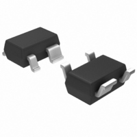
... Ordering Information Part Number No. of Devices ATF‑58143‑TR1G 3000 ATF‑58143‑TR2G 10000 ATF‑58143‑BLKG 100 Package Dimensions Outline 43 (SOT-343/SC70 4 lead) Notes: 1. All dimensions are in mm. 2. Dimensions are inclusive of plating. 3. Dimensions are exclusive of mold flash and metal blurr. 4. All specifications comply to EIAJ SC70. ...

Page 9

Tape Dimensions For Outline Description Cavity Length Width Depth Pitch Bottom Hole Diameter Perforlation Diameter Pitch Position Carrier Tape Width Thickness Cover Tape Width Thickness Distance Cavity to Perforation (Width Direction) ...

Related keywords