MRF6V2300NR1 Freescale Semiconductor, MRF6V2300NR1 Datasheet
MRF6V2300NR1
Specifications of MRF6V2300NR1
Available stocks


Related parts for MRF6V2300NR1

MRF6V2300NR1 Summary of contents
Page 1
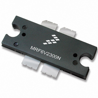
... CASE 1486- -03, STYLE 1 TO- -270 WB- -4 PLASTIC MRF6V2300NR1 CASE 1484- -04, STYLE 1 TO- -272 WB- -4 PLASTIC MRF6V2300NBR1 PARTS ARE SINGLE- -ENDED out out DS (Top View) Note: Exposed backside of the package is the source terminal for the transistor. Figure 1. Pin Connections Class 2 (Minimum) A (Minimum) IV (Minimum) MRF6V2300NR1 MRF6V2300NBR1 1 ...
Page 2
... Incorrect mounting can lead to internal temperatures which exceed the maximum allowable operating junction temperature. Refer to Freescale Application Note AN3263 (for bolt down mounting) or AN1907 (for solder reflow mounting) PRIOR TO STARTING SYSTEM DESIGN to ensure proper mounting of these devices. MRF6V2300NR1 MRF6V2300NBR1 2 Rating 3 = 25° ...
Page 3
... Z5 0.434″ x 0.220″ Microstrip Z6, Z7 0.298″ x 0.630″ Microstrip Figure 2. MRF6V2300NR1(NBR1) Test Circuit Schematic — 220 MHz Table 6. MRF6V2300NR1(NBR1) Test Circuit Component Designations and Values — 220 MHz Part B1 Ω, 100 MHz Long Ferrite Beads, Surface Mount B3 47 Ω, 100 MHz Short Ferrite Bead, Surface Mount C1 47 μ ...
Page 4
... C10 C11 C12 C13 * Stacked Figure 3. MRF6V2300NR1(NBR1) Test Circuit Component Layout — 220 MHz MRF6V2300NR1 MRF6V2300NBR1 4 C4 C19 C5 C18 C6 C17 R1 B2 C15* C8 C16 C20 L2 C14 L1 C23 C22 C21 MRF6V2300N/NB Rev Device Data Freescale Semiconductor ...
Page 5
... DRAIN--SOURCE VOLTAGE (VOLTS) DS Figure 5. DC Safe Operating Area I = 1350 Vdc 220 MHz 100 P , OUTPUT POWER (WATTS) CW out P3dB = 55.76 dBm (377 W) P1dB = 55.04 dBm (319 Vdc 900 220 MHz INPUT POWER (dBm) in MRF6V2300NR1 MRF6V2300NBR1 100 600 Ideal Actual 34 5 ...
Page 6
... P , OUTPUT POWER (WATTS) CW out Figure 10. Power Gain versus Output Power 160 Figure 13. VHF Broadcast Broadband Performance MRF6V2300NR1 MRF6V2300NBR1 6 TYPICAL CHARACTERISTICS 900 220 MHz 35 300 350 400 10 Figure 11. Power Output versus Power Input 25_C 85_C --30_C C 25_C 85_C η ...
Page 7
... T , JUNCTION TEMPERATURE (°C) J This above graph displays calculated MTTF in hours when the device is operated Vdc 300 W CW, and η DD out MTTF calculator available at http://www.freescale.com/rf. Select Software & Tools/Development Tools/Calculators to access MTTF calculators by product. 230 250 = 68%. D MRF6V2300NR1 MRF6V2300NBR1 7 ...
Page 8
... Figure 15. Series Equivalent Source and Load Impedance — 220 MHz MRF6V2300NR1 MRF6V2300NBR1 8 Z source f = 220 MHz Ω load f = 220 MHz Vdc 900 mA 300 out f Z source MHz Ω 220 1.23 + j3.69 2.43 + j2. Test circuit impedance as measured from source gate to ground Test circuit impedance as measured load from drain to ground ...
Page 9
... C20 C19 C15 L2*, R3*, ** C13 C12 Figure 16. MRF6V2300NR1(NBR1) Test Circuit Component Layout — 27 MHz Table 7. MRF6V2300NR1(NBR1) Test Circuit Component Designations and Values — 27 MHz Part B1 Ω, 100 MHz Long Ferrite Beads B2 47 Ω, 100 MHz Short Ferrite Bead C1 160 pF Chip Capacitor ...
Page 10
... C24 L1 Figure 17. MRF6V2300NR1(NBR1) Test Circuit Component Layout — 450 MHz Table 8. MRF6V2300NR1(NBR1) Test Circuit Component Designations and Values — 450 MHz Part B1 Ω, 100 MHz Long Ferrite Beads C1, C9, C17, C18 240 pF Chip Capacitors Chip Capacitor C3 47 μ Electrolytic Capacitor C4 22 μ Tantalum Capacitor C5 10 μ ...
Page 11
... Z = Test circuit impedance as measured from source gate to ground Test circuit impedance as measured from load drain to ground. Device Input Matching Under Test Network Z Z source load Z load Ω Output Matching Network MRF6V2300NR1 MRF6V2300NBR1 11 ...
Page 12
... MRF6V2300NR1 MRF6V2300NBR1 12 PACKAGE DIMENSIONS RF Device Data Freescale Semiconductor ...
Page 13
... RF Device Data Freescale Semiconductor MRF6V2300NR1 MRF6V2300NBR1 13 ...
Page 14
... MRF6V2300NR1 MRF6V2300NBR1 14 RF Device Data Freescale Semiconductor ...
Page 15
... RF Device Data Freescale Semiconductor MRF6V2300NR1 MRF6V2300NBR1 15 ...
Page 16
... MRF6V2300NR1 MRF6V2300NBR1 16 RF Device Data Freescale Semiconductor ...
Page 17
... RF Device Data Freescale Semiconductor MRF6V2300NR1 MRF6V2300NBR1 17 ...
Page 18
... MTTF” footnote added and changed 200°C to 225°C in Capable Plastic Package bullet • Added Electromigration MTTF Calculator and RF High Power Model availability to Product Software MRF6V2300NR1 MRF6V2300NBR1 18 REVISION HISTORY Description test condition to indicate AC stimulus on the V ...
Page 19
... Semiconductor was negligent regarding the design or manufacture of the part. Freescalet and the Freescale logo are trademarks of Freescale Semiconductor, Inc. All other product or service names are the property of their respective owners. © Freescale Semiconductor, Inc. 2007--2008, 2010. All rights reserved. MRF6V2300NR1 MRF6V2300NBR1 19 ...