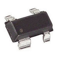
AT-41511-BLKG Avago Technologies US Inc., AT-41511-BLKG Datasheet - Page 3

AT-41511-BLKG
Manufacturer Part Number
AT-41511-BLKG
Description
TRANS NPN BIPO 12V 50MA SOT-143
Manufacturer
Avago Technologies US Inc.
Specifications of AT-41511-BLKG
Transistor Type
NPN
Voltage - Collector Emitter Breakdown (max)
12V
Noise Figure (db Typ @ F)
1dB ~ 1.7dB @ 900MHz ~ 2.4GHz
Gain
11dB ~ 15.5dB
Power - Max
225mW
Dc Current Gain (hfe) (min) @ Ic, Vce
30 @ 5mA, 5V
Current - Collector (ic) (max)
50mA
Mounting Type
Surface Mount
Package / Case
SOT-143, SOT-143B, TO-253AA
Transistor Polarity
NPN
Collector Emitter Voltage V(br)ceo
12V
Transition Frequency Typ Ft
10GHz
Power Dissipation Pd
225mW
Dc Collector Current
500mA
Dc Current Gain Hfe
270
Lead Free Status / RoHS Status
Lead free / RoHS Compliant
Frequency - Transition
-
Lead Free Status / RoHS Status
Lead free / RoHS Compliant, Lead free / RoHS Compliant
AT-41511, AT-41533 Typical Performance
Figure 1. AT-41511 and AT-41533 Minimum Noise
Figure vs. Frequency and Current at V
20
15
10
Figure 4. AT-41511 and AT-41533 Associated Gain
vs. Frequency and Current at V
Figure 7. AT-41511 and AT-41533 P
Frequency and Bias at V
Tuning.
3
5
0
0.1
20
15
10
3.0
2.5
2.0
1.5
1.0
0.5
5
0
10, 25 mA
10, 25 mA
0.1
0
0.1
0.6
5 mA
2 mA
5 mA
2 mA
FREQUENCY (GHz)
0.6
0.6
FREQUENCY (GHz)
1.1
FREQUENCY (GHz)
1.1
1.1
CE
1.6
= 2.7 V, with Optimal
PKG 11
PKG 33
1.6
CE
1.6
= 2.7 V.
2.1
1dB
CE
vs.
2.1
2.1
25 mA
10 mA
2, 5 mA
= 2.7 V.
2.6
25 mA
10 mA
5 mA
25
20
15
10
5
2.6
2.6
Figure 2. AT-41511 and AT-41533 Minimum Noise
Figure vs. Frequency and Current at V
Figure 5. AT-41511 and AT-41533 Associated Gain
vs. Frequency and Current at V
Figure 8. AT-41511 and AT-41533 P
Frequency and Bias at V
Tuning.
20
15
10
3.0
2.5
2.0
1.5
1.0
0.5
5
0
20
15
10
0.1
0
5
0
0.1
0.1
0.6
0.6
0.6
FREQUENCY (GHz)
FREQUENCY (GHz)
PKG 11
PKG 33
FREQUENCY (GHz)
1.1
1.1
1.1
CE
= 5 V, with Optimal
1.6
1.6
CE
1.6
= 5 V.
1dB
2.1
CE
vs.
2.1
= 5 V.
2.1
10 mA
25 mA
2 mA
5 mA
25 mA
10 mA
10, 25 mA
10, 25 mA
5 mA
5 mA
5 mA
2.6
2.6
2.6
Figure 3. AT-41511 and AT-41533 Minimum Noise
Figure vs. Frequency and Current at V
Figure 6. AT-41511 and AT-41533 Associated Gain
vs. Frequency and Current at V
Figure 9. AT-41511 and AT-41533 P
Frequency and Bias at V
Tuning.
20
15
10
3.0
2.5
2.0
1.5
1.0
0.5
20
15
10
5
0
5
0
0
0.1
0.1
0.1
0.6
0.6
0.6
FREQUENCY (GHz)
FREQUENCY (GHz)
FREQUENCY (GHz)
PKG 11
PKG 33
1.1
1.1
1.1
CE
= 8 V, with Optimal
1.6
1.6
CE
1.6
= 8 V.
1dB
CE
2.1
vs.
2.1
2.1
= 8 V.
25 mA
10 mA
5 mA
25 mA
10 mA
5 mA
10, 25 mA
10, 25 mA
5 mA
5 mA
2.6
2.6
2.6


