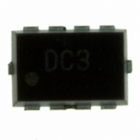
ZXTDC3M832TA Diodes Zetex, ZXTDC3M832TA Datasheet - Page 2

ZXTDC3M832TA
Manufacturer Part Number
ZXTDC3M832TA
Description
TRANS NPN 50V PNP 40V 8MLP
Manufacturer
Diodes Zetex
Datasheet
1.ZXTDC3M832TA.pdf
(8 pages)
Specifications of ZXTDC3M832TA
Transistor Type
NPN, PNP
Current - Collector (ic) (max)
4A, 3A
Voltage - Collector Emitter Breakdown (max)
50V, 40V
Vce Saturation (max) @ Ib, Ic
320mV @ 200mA, 4A / 370mV @ 250mA, 2.5A
Current - Collector Cutoff (max)
25nA
Dc Current Gain (hfe) (min) @ Ic, Vce
100 @ 2A, 2V / 60 @ 1.5A, 2V
Power - Max
1W
Frequency - Transition
165MHz, 190MHz
Mounting Type
Surface Mount
Package / Case
8-MLP
Lead Free Status / RoHS Status
Lead free / RoHS Compliant
Other names
ZXTDC3M832TATR
Available stocks
Company
Part Number
Manufacturer
Quantity
Price
Company:
Part Number:
ZXTDC3M832TA
Manufacturer:
ZETEX
Quantity:
9 000
ABSOLUTE MAXIMUM RATINGS.
THERMAL RESISTANCE
Notes
(a) For a dual device surface mounted on 8 sq cm single sided 2oz copper on FR4 PCB, in still air conditions with all exposed pads attached. The
copper area is split down the centre line into two separate areas with one half connected to each half of the dual device.
(b) Measured at t<5 secs for a dual device surface mounted on 8 sq cm single sided 2oz copper on FR4 PCB, in still air conditions with all exposed
pads attached. The copper area is split down the centre line into two separate areas with one half connected to each half of the dual device.
(c) For a dual device surface mounted on 8 sq cm single sided 2oz copper on FR4 PCB, in still air conditions with minimal lead connections only.
(d) For a dual device surface mounted on 10 sq cm single sided 1oz copper on FR4 PCB, in still air conditions with all exposed pads attached
attached. The copper area is split down the centre line into two separate areas with one half connected to each half of the dual device.
(e) For a dual device surface mounted on 85 sq cm single sided 2oz copper on FR4 PCB, in still air conditions with all exposed pads attached
attached. The copper area is split down the centre line into two separate areas with one half connected to each half of the dual device.
(f) For a dual device with one active die.
(g) For dual device with 2 active die running at equal power.
(h) Repetitive rating - pulse width limited by max junction temperature. Refer to Transient Thermal Impedance graph.
(i) The minimum copper dimensions required for mounting are no smaller than the exposed metal pads on the base of the device as shown in the
package dimensions data. The thermal resistance for a dual device mounted on 1.5mm thick FR4 board using minimum copper 1 oz weight, 1mm
wide tracks and one half of the device active is Rth = 250°C/W giving a power rating of Ptot = 500mW.
ZXTDC3M832
PARAMETER
Collector-Base Voltage
Collector-Emitter Voltage
Emitter-Base Voltage
Peak Pulse Current
Continuous Collector Current (a)(f)
Base Current
Power Dissipation at TA=25°C (a)(f)
Linear Derating Factor
Power Dissipation at TA=25°C (b)(f)
Linear Derating Factor
Power Dissipation at TA=25°C (c)(f)
Linear Derating Factor
Power Dissipation at TA=25°C (d)(f)
Linear Derating Factor
Power Dissipation at TA=25°C (d)(g)
Linear Derating Factor
Power Dissipation at TA=25°C (e)(g)
Linear Derating Factor
Operating and Storage Temperature Range
PARAMETER
Junction to Ambient (a)(f)
Junction to Ambient (b)(f)
Junction to Ambient (c)(f)
Junction to Ambient (d)(f)
Junction to Ambient (d)(g)
Junction to Ambient (e)(g)
SYMBOL
V
V
V
I
I
I
P
P
P
P
P
P
T
SYMBOL
R
R
R
R
R
R
CM
C
B
CBO
CEO
EBO
D
D
D
D
D
D
j
:T
JA
JA
JA
JA
JA
JA
stg
2
NPN
100
7.5
50
6
4
-55 to +150
VALUE
1000
2.45
19.6
1.13
13.6
83.3
73.5
41.7
1.5
1.7
125
111
12
24
51
1
8
9
3
PNP
-7.5
-50
-40
-4
-3
ISSUE 1 - JUNE 2002
mW/°C
mW/°C
mW/°C
mW/°C
mW/°C
mW/°C
UNIT
UNIT
°C/W
°C/W
°C/W
°C/W
°C/W
°C/W
mA
W
W
W
W
W
W
°C
V
V
V
A
A


