74ABT125D NXP Semiconductors, 74ABT125D Datasheet
74ABT125D
Specifications of 74ABT125D
Available stocks


Related parts for 74ABT125D


74ABT125D Summary of contents
Page 1
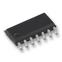
... Ordering information Type number Package Temperature range 40 C to +85 C 74ABT125N 40 C to +85 C 74ABT125D 40 C to +85 C 74ABT125DB 40 C to +85 C 74ABT125PW 40 C to +85 C 74ABT125BQ Name Description DIP14 plastic dual in-line package; 14 leads (300 mil) SO14 plastic small outline package ...
Page 2
... NXP Semiconductors 4. Functional diagram 1OE 2OE 3OE 4OE 13 mna228 Fig 1. Logic symbol 5. Pinning information 5.1 Pinning 74ABT125 1OE 2OE GND 7 Fig 4. Pin configuration DIP14, SO14 and (T)SSOP14 74ABT125 Product data sheet EN1 mna229 Fig 2. IEC logic symbol 4OE 3OE 001aai027 Fig 5. ...
Page 3
... NXP Semiconductors 5.2 Pin description Table 2. Pin description Symbol Pin 1OE to 4OE GND Functional description [1] Table 3. Function selection Inputs nOE [ HIGH voltage level LOW voltage level don’t care high-impedance OFF-state. 7. Limiting values [1] Table 4. Limiting values In accordance with the Absolute Maximum Rating System (IEC 60134). ...
Page 4
... NXP Semiconductors 8. Recommended operating conditions Table 5. Operating conditions Voltages are referenced to GND (ground = 0 V). Symbol Parameter V supply voltage CC V input voltage I V HIGH-level input voltage IH V LOW-level Input voltage IL I HIGH-level output current OH I LOW-level output current OL t/V input transition rise and fall rate ...
Page 5
... NXP Semiconductors Table 6. Static characteristics Symbol Parameter I additional supply CC current C input capacitance I C output capacitance O [1] This parameter is valid for any V a transition time 100 s is permitted. [2] Not more than one output should be tested at a time, and the duration of the test should not exceed one second. ...
Page 6
... NXP Semiconductors 11. Waveforms and V are typical voltage output levels that occur with the output load Fig 6. Propagation delay input (nA) to output (nY) nOE input output LOW-to-OFF OFF-to-LOW output HIGH-to-OFF OFF-to-HIGH and V are typical voltage output levels that occur with the output load. ...
Page 7
... NXP Semiconductors negative V M pulse positive V M pulse Input pulse definition Test data is given in Table Test circuit definitions Load resistance Load capacitance including jig and probe capacitance Termination resistance should be equal to output impedance Test voltage for switching times. EXT Fig 8. Load circuitry for switching times Table 8 ...
Page 8
... NXP Semiconductors 12. Package outline DIP14: plastic dual in-line package; 14 leads (300 mil pin 1 index 1 DIMENSIONS (inch dimensions are derived from the original mm dimensions UNIT max. min. max. mm 4.2 0.51 3.2 inches 0.17 0.02 0.13 Note 1. Plastic or metal protrusions of 0.25 mm (0.01 inch) maximum per side are not included. ...
Page 9
... NXP Semiconductors SO14: plastic small outline package; 14 leads; body width 3 pin 1 index 1 e DIMENSIONS (inch dimensions are derived from the original mm dimensions) A UNIT max. 0.25 1.45 mm 1.75 0.25 0.10 1.25 0.010 0.057 inches 0.069 0.01 0.004 0.049 Note 1. Plastic or metal protrusions of 0.15 mm (0.006 inch) maximum per side are not included. ...
Page 10
... NXP Semiconductors SSOP14: plastic shrink small outline package; 14 leads; body width 5 pin 1 index 1 e DIMENSIONS (mm are the original dimensions) A UNIT max. 0.21 1. 0.25 0.05 1.65 Note 1. Plastic or metal protrusions of 0.25 mm maximum per side are not included. OUTLINE VERSION IEC SOT337-1 Fig 11. Package outline SOT337-1 (SSOP14) ...
Page 11
... NXP Semiconductors TSSOP14: plastic thin shrink small outline package; 14 leads; body width 4 pin 1 index 1 e DIMENSIONS (mm are the original dimensions) A UNIT max. 0.15 0.95 mm 1.1 0.25 0.05 0.80 Notes 1. Plastic or metal protrusions of 0.15 mm maximum per side are not included. 2. Plastic interlead protrusions of 0.25 mm maximum per side are not included. ...
Page 12
... NXP Semiconductors DHVQFN14: plastic dual in-line compatible thermal enhanced very thin quad flat package; no leads; 14 terminals; body 2 0.85 mm terminal 1 index area terminal 1 index area DIMENSIONS (mm are the original dimensions) (1) A UNIT max. 0.05 0. 0.2 0.00 0.18 Note 1. Plastic or metal protrusions of 0.075 mm maximum per side are not included. ...
Page 13
... NXP Semiconductors 13. Abbreviations Table 9. Abbreviations Acronym Description BiCMOS BipolarCMOS DUT Device Under Test ESD ElectroStatic Discharge HBM Human Body Model MM Machine Model 14. Revision history Table 10. Revision history Document ID Release date 74ABT125 v.5 20101124 • Modifications: Figure note [1] 74ABT125 v.4 20100427 74ABT125 v.3 20080429 74ABT125 v ...
Page 14
... In no event shall NXP Semiconductors be liable for any indirect, incidental, punitive, special or consequential damages (including - without limitation - lost profits, lost savings, business interruption, costs related to the removal or ...
Page 15
... NXP Semiconductors Export control — This document as well as the item(s) described herein may be subject to export control regulations. Export might require a prior authorization from national authorities. 16. Contact information For more information, please visit: For sales office addresses, please send an email to: 74ABT125 Product data sheet 15 ...
Page 16
... NXP Semiconductors 17. Contents 1 General description . . . . . . . . . . . . . . . . . . . . . . 1 2 Features and benefits . . . . . . . . . . . . . . . . . . . . 1 3 Ordering information . . . . . . . . . . . . . . . . . . . . . 1 4 Functional diagram . . . . . . . . . . . . . . . . . . . . . . 2 5 Pinning information . . . . . . . . . . . . . . . . . . . . . . 2 5.1 Pinning . . . . . . . . . . . . . . . . . . . . . . . . . . . . . . . 2 5.2 Pin description . . . . . . . . . . . . . . . . . . . . . . . . . 3 6 Functional description . . . . . . . . . . . . . . . . . . . 3 7 Limiting values Recommended operating conditions Static characteristics Dynamic characteristics . . . . . . . . . . . . . . . . . . 5 11 Waveforms . . . . . . . . . . . . . . . . . . . . . . . . . . . . . 6 12 Package outline . . . . . . . . . . . . . . . . . . . . . . . . . 8 13 Abbreviations ...